The inspiration for this series of articles came from Microchip’s TB3103 and TB3104 , which outlined the implementation of current mode controlled buck and boost converters using the PIC16F753’s internal analog peripherals, which include an operational amplifier, a comparator, PWM, etc.
As a hobbyist, I’ve always found stuff like transfer functions, bode plots (the more complex ones), and SPICE to be really intimidating. I am aware of what these are, and why they are used in circuit design, but I’ve never really sat down and worked with them before, much less explore their nitty gritty details.
Seeing that I have a bunch of MCP6004 op amps left over from a demo session I gave in my high school physics class, I figured that it was prime time I patch this gaping hole in my electronics knowledge. So here we are, about to kick off an exploration into the fundamentals of switched mode power converters (or switchmode, for some reason I have always thought “switchmode” is the term everyone uses, Wikipedia has other ideas however, and so I’m rolling with it).
I imagine that this is going to be one exhilarating journey, and I’d like to bring you along. The plan is to break a basic boost converter into its fundamental building blocks, design fully analog circuits to carry out those functions, work out the math behind everything, and hopefully by the end be left with a working boost converter. If I manage to get at least a semi functional boost converter before university starts, then I might even look at some ways of optimising the design by giving it better transient response, better efficiency and all that good stuff. Read: more maths and formulae.
And if I’m really really lucky, I may even have time to explore other topologies, and also experiment with current mode control designs.
The plan, for now
Why a boost converter? Well, the MCP6004 is a low voltage op amp that only goes up to 6V. Thus, I am opting use 4 AA batteries to power this entire experiment as it eliminates the possibility of silly ol’ me shorting stuff out with my oscilloscope ground and blowing stuff up. I don’t really think there is much point in reducing that 6V even further, so boost converter it is.
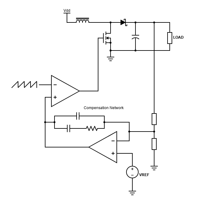
Here’s a block diagram of the boost converter I’m planning to build:
Garden variety boost converter schematic: it doesn’t get more rudimentary than this
Garden variety boost converter schematic: it doesn’t get more rudimentary than this
To keep things simple, I am going to be starting off with voltage mode control. Since the MCP6004 is kinda slow, and the entire thing will probably be built on a breadboard, I’m keeping the switching frequency nice and slow, in the 10s of kHz range. My hope is that this will somewhat limit oscillations and other instabilities.
For me, the design of the compensation network is the highlight of this entire exercise. But, since this design is going to be inherently slow, I don’t know if its even going to be necessary at all. At any rate, I do have some better op amps coming (NCS20034 and MCP6477, both substantially faster parts), so I’ll be able to crank the frequency up and experiment with compensation networks if the preliminary experiments succeed.
This is probably going to be the crappiest boost converter in the history of boost converters. Its probably going to have terrible efficiency, slow transient response, and overall just not regulate very well at all. But in some ways that’s kinda what I’m going for, since a lot of the math and simulations and plots have to do with optimising these parameters, and well, I think we can all agree its a heck of a lot easier to optimise a crappy design into a passable one, rather than trying to squeeze out every last ounce of performance from a robust design.
Roadmap
For the record, I want to go ahead and throw my ideas for where this adventure is going to go once I get the crap version above to work.
- Make it faster: increase the switching frequency of the design to the hundreds of kHz at the very least
- Make it efficient. It doesn’t have to be like 80+ titanium or anything; it just has to not suck
- Synchronous rectification.
- Current mode control. This is a big one too, the two appnotes that inspired this saga are peak current mode control converters. Before reading them I’ve never even heard about current mode control, and I’d like to take this opportunity to explore how these different schemes work and potentially compare them side by side.
- Build the end result on perfboard and characterize it. Again, not hoping for anything groundbreaking here, I just want to explore this area of engineering. The only piece of equipment I have available is the venerable Rigol DS1054z, I’ll see how far it can take me on this journey.
- SPICE the whole thing to see what this SPICE thing is all about.
- Designing a PCB for it and optimising the layout. This one’s pretty remote, seeing that COVID is currently in full force, and I have less than 2 months until university begins. We’ll see soon enough
Getting a little sentimental: a small glimpse of my background, and why you should have an oscilloscope
Analog circuitry (specifically audio electronics) was what got me into electronics in the first place, but after all these years, I still feel like I never properly learned what goes into designing circuits that perform well, much less get familiar with good PCB layout practices for low noise and distortion.
My biggest mistake in exploring electronics is definitely, without question, not getting an oscilloscope early on. So many projects were never finished because they didn’t work, and I didn’t know, couldn’t know why. Trying to make audio equipment, even if its just building off schematics online, without an oscilloscope really is like prodding about in the dark: I didn’t know what I was doing. The worst bit: all those failures were precious opportunities to go down rabbit holes and learn, and I let them slide!
So, if you are a hobbyist (as I should presume you are, since you’re reading this), especially if you’re just starting out and are serious about actually learning electronics, Get. An. Oscilloscope. Not one of those DSO138 shenanigans, get a real benchtop scope, even if its something like a Hantek. If possible, go for one with 4 channels, it makes seeing the whole picture so much easier.
I hope all this is about to change, and that in bringing you along with me on this journey, at the very least you’ll gain what I sorely lacked for the past decade as an electronics hobbyist: confidence to tinker and explore.
This series of articles is going to be freeform and spontaneous, almost like lab notes. I want to show you as many of the paths I took as possible, mistakes included. I will also try to present all the math that I’ve done, even if its done after I arrive at a working design by trial and error. I feel like I’m not familiar enough with all those formulae to design circuits with them, but IMO verifying that the math matches with real life circuit characteristics will allow me to learn a lot and get comfortable with it. I will attempt to keep all the math in a separate section in each article in case you want to skip it.
Bon voyage!