With the addition of these 3 components, I had a fully functional boost converter! However, it is not without its (huge) caveats, and let’s just say that along the way, Murphy has paid me many, many visits.
In Chapter 1 , we talked about the sawtooth generator, which connects directly to the an opamp responsible for generating a PWM gate drive signal. So, I thought it made sense to take a closer look at that next.
PWM Modulator
This bit of the circuit is nothing more than a comparator. As a proof of concept, I first hooked up a potentiometer as the control voltage source.
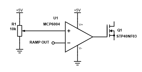
And that was literally it, I got a beautiful PWM at the output of the opamp, whose duty cycle is proportional to the input control voltage.
Power Stage
Next, I proceeded to wire up the output stage, which is a really basic boost converter output stage configuration. Note that all the component values here are completely arbitrary, they are randomly selected from my parts bin. We’ll explore the proper design procedure in which all the component values are calculated according to the design goals in a later part.
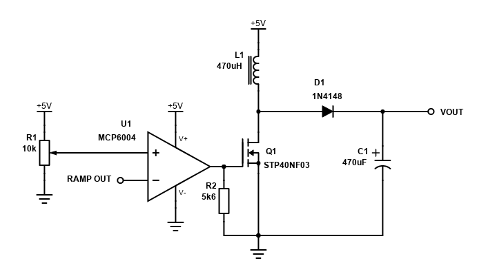
Yes, that is a 1N4148 small signal diode. It was the only type of through hole diode I had laying around, and I’m not going to be experimenting with heavy currents (yet) anyways.
R2 is there to act as a pull down for the MOSFET’s gate. It probably isn’t necessary since the output of the opamp is low impedance, but I figured the extra safety wouldn’t hurt.
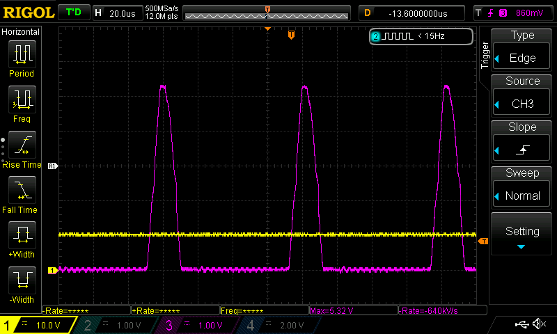
Right now, this circuit alone is technically a boost converter. Although since there is absolutely no feedback loop it is completely unregulated. But, if we power it up, it should be able to output a voltage that is higher than the supply voltage of 5V.
And indeed, it does. Here I have a 1kΩ resistor hooked up to the output as a light load to stabilise things.
With a higher duty cycle, ie a higher control voltage.
With a lower duty cycle, ie a lower control voltage.
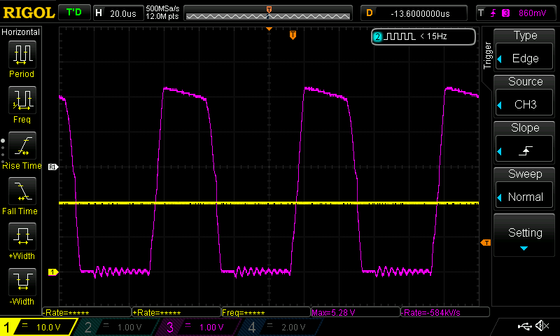
As you can see, the output voltage is well into the range of 10’s of volts. Great! But now watch what happens when I swap out the 1kΩ resistor for a 330Ω one:
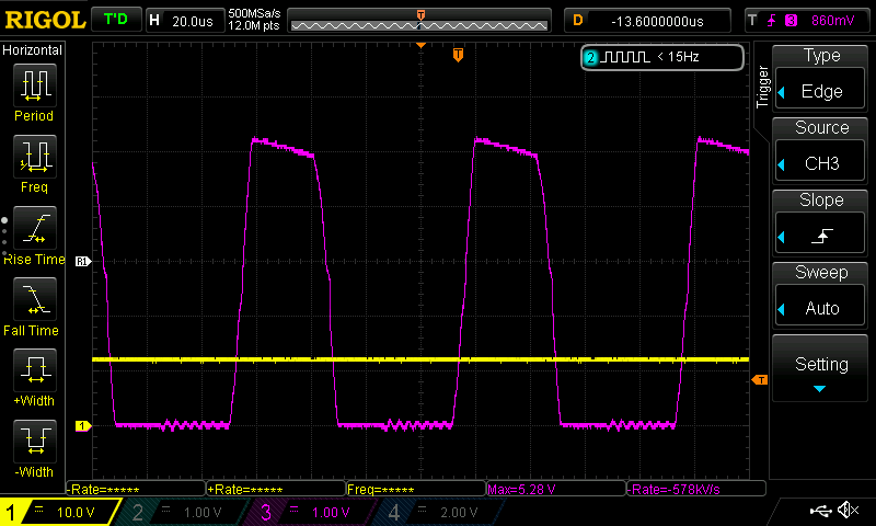
Just by changing the load, the output voltage has fallen from around 20V to something like 12V, not great…
What it needs now is a feedback loop, that will constantly monitor the output voltage and change the duty cycle to keep the voltage steady at a value that we can set.
Error Amp
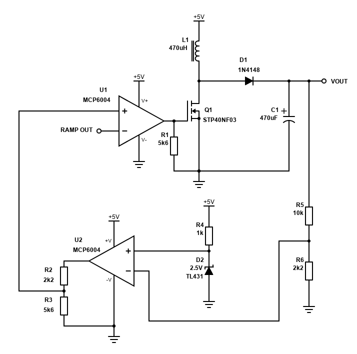
Digikey Scheme-it does not have a symbol for the TL431… but its essentially like a zener in this configuration anyways.
The error amp is basically the entire bottom part of the schematic. Since the error amp is, well, an opamp, it will “try” (sorry for anthropomorphising) to keep the voltage level at its 2 inputs the same. So, in this context, it varies its output voltage so as to control the duty cycle to maintain the voltage at its inverting input at a steady 2.5V.
The output voltage will thus be whatever voltage that yields 2.5V through the resistor divider consisting of R5 and R6, and is given by the formula:
$$V_{OUT} = (1+\frac{R5}{R6}) \times 2.5V$$
In this case, its around 13.84V, taking into account resistor tolerances.
And there we have it! A working boost converter that actually regulates.
Discussion
Duty cycle limiting
Straight off the bat, I want to bring your attention to R2 and R3 in the final schematic above.
Initially, I didn’t think of adding anything like that. However, that quickly proved to literally be fatal, as I magic smoke and a burned finger were the scars of Murphy’s onslaught.
Without them, basically what happens when the entire circuit is first starting up is the output is obviously at 0V, while the TL431 has already started to regulate at 2.5V. Thus, the error amp’s output will swing high. Recall from chapter 1 that the maximum voltage the ramp generator reaches is just a little over 4V. So, if the error amp is outputting 5V, the PWM basically never starts, and the gate of the MOSFET is held high.
Read: The MOSFET shorts the supply rail to ground…
And since the MOSFET never switches, the voltage never gets boosted, and basically there is no mechanism to get ourselves out if this sticky situation.
I quickly came up with the idea to just scale down the error amp output using a voltage divider, that way no matter what the output will be some sort of PWM waveform. I chose values that wouldn’t limit the duty cycle too much, but it turns out that was not really an issue at all.
I’m not sure if that’s how they do it in proper non amateur implementations, and I’m also unsure of how it affects the loop gain and phase margin and all the nerdy maths stuff. Maybe in a future part of this series I’ll revisit this tangled mess.
Determining which opamp input to connect stuff to
I’m not gonna lie, in the outline page , I just copied that diagram from the internet without much thought. So when it came to implementing the actual circuit, I resorted to use some wacky mental reasoning to determine which way round should I connect the feedback signal and the reference signal to the error amp, and subsequently which way round do I connect the sawtooth waveform and the error amp output to the PWM modulator part.
I don’t know how accurate it is, but the end result worked, and so hopefully it helps you too.
It goes like this:
To keep stuff intuitive, I want the PWM modulator to respond to an increase in voltage with an increase in duty cycle, so the ramp must be connected to the inverting input.
Now, lets say the voltage out of the feedback divider is lower that the 2.5V reference. The circuit should respond by increasing power delivered to the output, i.e. by storing more energy in the inductor (and thus releasing more energy in the spike) and thus increasing the duty cycle.
I.e. if the voltage is too low, I want the error amp output to go higher.
Thus, the feedback signal, which is lower than the reference signal, should be connected to the inverting input; and the reference to the non-inverting input.
Quick sanity check in the case that the voltage goes higher than the desired output also holds according to this logic.
My brain
Inductive spiking
Just for fun, I wanted to take a look at what the waveform at the drain looked like without the smoothing capacitor. Using the circuit sans the error amp , I removed the load and the output smoothing capacitor, and had a look at that inductive spiking (or back EMF).
Almost 40V peaks, cool!
Discontinuous current mode
DISCLAIMER: The following is my very limited understanding of discontinuous and continuous current modes. Take what you will and leave the rest.
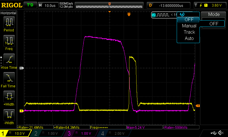
So basically, I was poking around and decided to probe the drain voltage of the FET.
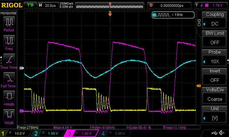
Ch1: Drain voltage; Ch2: Error amp output, Ch3: Gate voltage
Notice all those squiggles? I thought great! We have some oscillations going on, now I have an excuse to do some loop compensation experiments.
Then for whatever reason, I decided to touch the tab of the FET (which is the drain) and it got suppressed, suggesting that it indeed was some sort of parasitic capacitance stuff. To my inexperienced brain, parasitic capacitances -> opamp oscillation -> loop compensation.
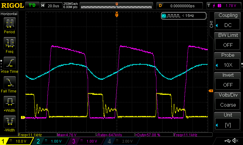
But nope, turns out that after some Google-fu, this is a hallmark of Discontinuous Current Mode in switching regulators.
Basically, there is Continuous Current Mode (CCM), and there is Discontinuous Current Mode (DCM) (NOT dichloromethane… damn chemistry…).
Under normal circumstances, switching regulators should operate under CCM, where there is a constant flow of current through the inductor. However if the load is very light and your design (my design) is not optimised for that; or if the load is highly dynamic and suddenly decides to switch into some low power state, the inductor current can fall completely to 0 as no more energy is being pulled out of it. The switching regulator enters DCM.
In DCM, the inductor essentially still has energy left. So, it forms an LC tank with all the parasitic capacitances of the PCB, surrounding semiconductors and such and resonates, which shows up as those oscillations. I read somewhere that if EMI isn’t an issue, one could just leave it at that, but efficiency is going to suffer since the oscillating voltage incurs I2R losses.
One way to suppress this is by using an RC snubber. I’ll get to messing around with that if the issue persists in subsequent revisions.
Math
Really, the only thing worth mentioning is the derivation of the formula for the output voltage .
We want a voltage of 2.5V to be present across R6. Therefore:
$$\begin{align*}V_{REF} &= \frac{R6}{R5+R6} \times V_{OUT} \newline \Rightarrow V_{OUT} &= \frac{R5 + R6}{R6} \times V_{REF} \newline &= (1+\frac{R5}{R6}) \times V_{REF} \newline &= (1+\frac{R5}{R6}) \times 2.5V \end{align*} \newline$$
It is very similar to the formula of the super duper ubiquitous LM317, because the LM317 also works in similar manner. Basically, it maintains a voltage of 1.23V across its Vout and Adj pins.
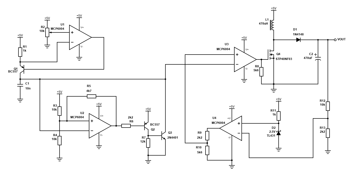
Complete schematic thus far
Just for the sake of completeness, here is the entire circuit in one diagram. Please note that the component designations will be different because well.. Digikey Scheme-it…