Being on a little analog synth nerd-out lately, I chose to kick things off by designing the sawtooth generator that will ultimately determine the switching frequency of the boost converter.
The sawtooth wave generated is used to derive the PWM signal that drives the gate of the FET. By connecting it and a control voltage to a comparator, a PWM signal with a duty cycle directly proportional to the control voltage will be generated.
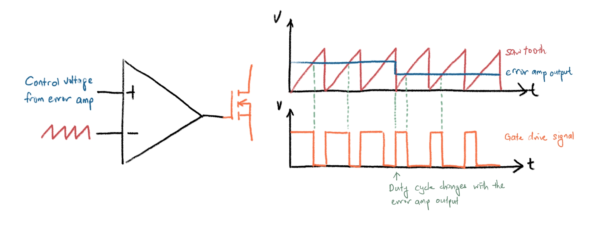
How a sawtooth wave can be used to derive a PWM signal based on a given control voltage
There are two parts to a sawtooth wave: the linear ramp up, and the quick snap down to ground (or whatever lowest voltage desired). So, in order to generate a sawtooth wave using opamps, a good place to start would be to tackle these two parts individually. There are quite a number of sawtooth generator circuits floating around on the internet, many of them based on opamp integrators. However, in testing those I just could not get them to behave nicely with my cobbled-together breadboard circuit. Instead, I drew some inspiration from this circuit from Maxim.
Linear ramp
If you’re familiar with basic capacitor theory, you’ll know that the rate of change of the voltage across a capacitor is directly proportional to the current flowing through the capacitor. Or in other words:
$$\require{amssymb} I = C \frac{dv}{dt} \ \Rightarrow\frac{dv}{dt} = \frac{I}{C}$$
If you’re uncomfortable with this, just know that if you charge the capacitor with a constant current, the voltage across its terminals will increase linearly with time, same goes for discharging.
I devised a pretty simple constant current source to achieve this.
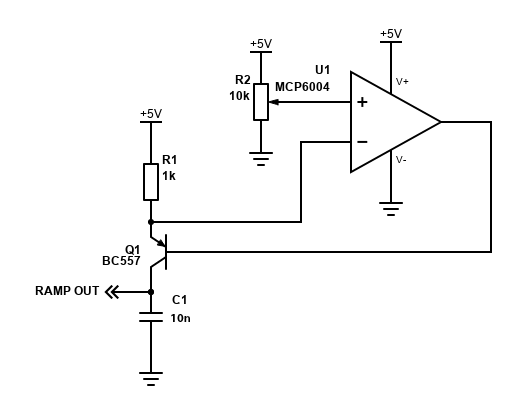
This circuit is pretty similar to the one in the Maxim appnote. The main differences being that I changed the low side current sensing to high side current sensing so that I can have my capacitor referenced to ground. This simplifies the design of the discharging part of the circuit. I also didn’t want to have to deal with bipolar supplies either.
The opamp regulates the voltage at the emitter of Q1 to be the same as whatever voltage is present on its non-inverting input. In doing so it maintains a constant voltage across R1, which in turn means that a constant current flows through R1 and thus through C1, producing the linear ramp.
The pot is just there to make it easier to change the rate at which the capacitor is charged, which controls the frequency of the resulting sawtooth wave.
Discharging the capacitor
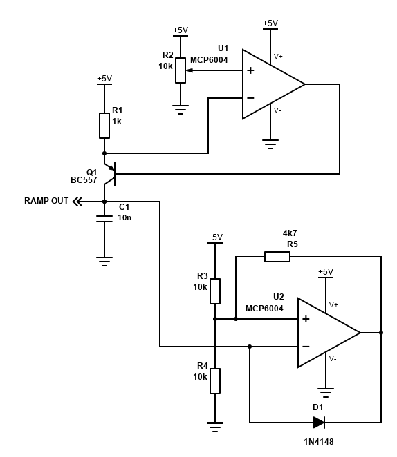
Now, we need to tack on a circuit that will discharge the capacitor when it reaches a certain voltage, so it can start charging all over again and we get a sawtooth wave.
The following circuit is going to be a little strange, since I was adapting the circuit from the Maxim appnote, and needed to invert the output of the opamp to get the correct discharging behavior.
Yes, the comparator can be wired up in a non-inverting configuration, but then its input impedance will be much lower and that’s gonna cause issues with the ramp generator, since the ramp generator charges the capacitor with several hundred nanoamps only.
U2 is wired up as a Schmitt trigger, its output goes low when the voltage at the inverting input exceeds the upper threshold voltage, here, that’s about 3.8V. This turns on Q2, which subsequently turns on Q3 and rapidly discharges C1. This produces the steep drop in voltage we were talking about.
Then, as the voltage of the capacitor falls below the lower threshold, here about 1.2V, the Schmitt trigger fires again, this time its output swings high, turning off Q2 and Q3. The upper and lower threshold voltages are set by R3, R4 and R5, the math for that will be below.
R6 limits the base current flowing into Q2 to prevent the circuit from self destructing. R7 is just an arbitrary high-ish value pulldown resistor to make sure Q3 is off when its supposed to be off. The value of 12k isn’t really critical in this application, I just happen to have a 12k resistor laying on the bench.
One interesting note is that Q2 and Q3 are wired up in what’s essentially a Sziklai pair. The combination of Q2 and Q3 acts as a PNP transistor. Like a Darlington pair (which I think many more of you are familiar with, I certainly didn’t learn of the Sziklai pair till much later), the Sziklai pair increases the overall current gain. It is probably unnecessary in this circuit, but hey, I first started with the idea of using an NPN to discharge C1, and only thought to use the PNP as an inverter to get the polarity right. Just Q2 probably would have worked just as well.
So, overall I’ve essentially built myself a crude VCO (voltage controlled oscillator). Its frequency is solely determined by the rate at which C1 charges.
Discussion
Now you might be thinking, especially if you’ve checked out the Maxim appnote, why don’t just discharge the capacitor with the opamp itself? Well, its because the MCP6004 is a slow opamp. With its slew rate of 0.6v/us the resulting wave is less like a sawtooth and more like a lopsided triangle wave. Plus, you’ll need a diode between the output of the opamp and the capacitor to prevent the opamp itself from charging the capacitor, which causes weird stuff to happen too.
Something like this discharges the capacitor directly through the opamp’s output stage
The output waveform of a configuration similar to the Maxim appnote
Notice how slowly the voltage is dropping? That’s due to the slew rate limit of the opamp limiting the rate at which its output voltage can change. Here, its -0.598V/us, close enough to the 0.6V/us in the datasheet.
Also note how the tops of the peaks are rounded over? Basically, I think this is because the capacitor is discharged through a diode (I used a 1N4148). When the comparator trips, the opamp’s output has to swing down from 5V. However, because of the slew rate it takes a while to get there, and when it does, it still has to swing an additional 0.7V diode drop. I think the rounded bit starts when the opamp’s output is at the same voltage as the capacitor, and the diode is just starting to get forward biased. Since we’re dealing with tiny currents (in the nA range) here any leakages through the diode beyond the capacitor charge current, before it is fully turned on starts to discharge the capacitor in a non linear way. Thus, the tops of the wave are rounded over.
With the transistor output stage, things look much much sharper.
Don’t mind the change in frequency, I was fiddling around. However you may now notice that the upper trip threshold is different, and the wave extends below ground.
I have no idea why these two things occur. My guess for the upper trip threshold would be that the opamp is actually tripping correctly, but once again due to its slow slew rate, there is a significant delay between when the comparator trips and when the transistors discharge the capacitor, allowing the capacitor voltage to continue to rise.
As for the part that goes below ground, I think it’s due to the fact that I’m using a crappy breadboard that came in one of those Arduino kits. It just doesn’t make good contact with the skinny legs on my cheap generic chinese resistors. I first thought that it was some sort of return current interference thing, so I rewired all the grounds on the breadboard to a star ground configuration to try to fix that. No luck, the circuit just did more weird stuff with the ground level jumping all over the place.
Then I kinda poked some of the resistors and the problem went away… Now I could not reproduce this issue no matter what I do. Well, so ends the trail on this then…
But wait! There’s more!
In investigating this ground reference level thing, I started probing at various nodes in the circuit, including the base of the PNP output transistor, and well, lets just say things got weirder…
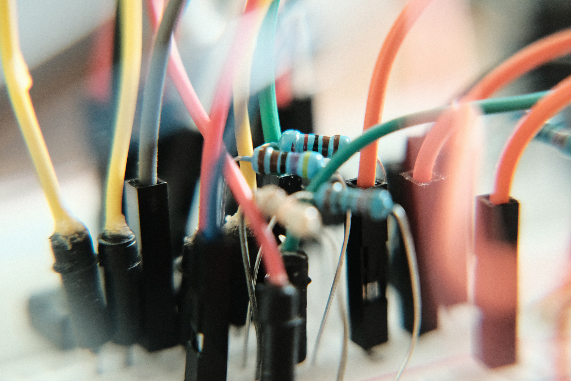
Take a look at the breadboard setup. Yes, I do realise that it is an absolute atrocity of a ratsnest.
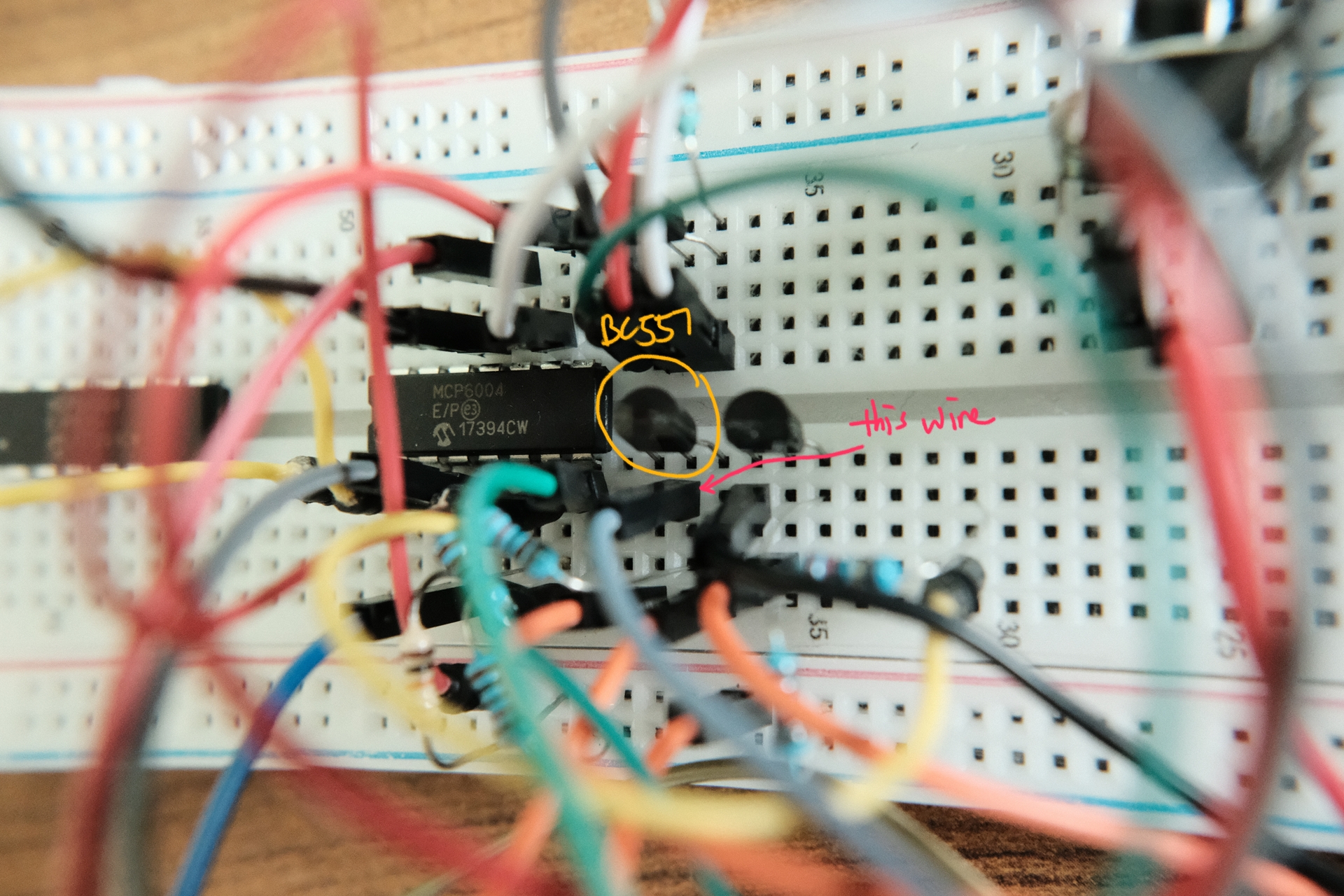
I’d like to bring your attention to the wire connected to the base (middle) pin of the BC557 PNP transistor.
I was trying to figure out what the opamp was doing at its output and why did the ground level of the output signal seem to have a mind of its own, one of the nodes I decided to check was this base pin, and I have a probe off screen hooked up to that grey jumper wire.
This is what I saw on the scope.
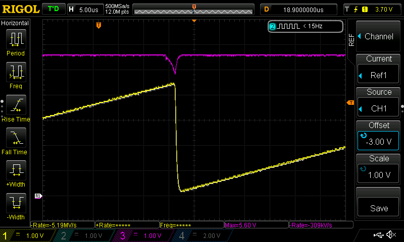
Channel 3 (Magenta) is connected to the output pin of the opamp, channel 1 is connected to the “positive” terminal of the 10nF capacitor.
Channel 2 is hooked up to the grey wire, but its turned off at the moment to avoid clutter.
Now, look what happens when I unplug that grey wire.
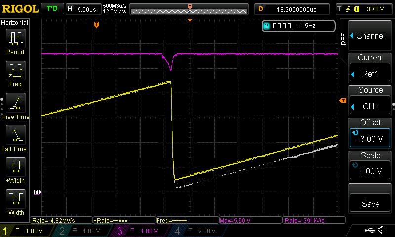
The white trace is a reference waveform from above
Whoa, that’s one sick puppy…
After some poking around, I got frustrated and really confused. So I decided to disconnect the Channel 2 probe at the scope. Here’s the result:

It is ever so slightly higher than the reference trace, suggesting that the lowering of this trace is due to the probe wire just being there.
I did some more poking about, and finally decided to unclip the probe from the grey jumper wire. And guess what, the waveform didn’t change at all! It was only when I pulled the wire out of the breadboard the trace changed in any significant way.
So the jumper wire just being there is causing all this…what?! I seriously have no idea why this is happening. My only guess would be that the clips inside the breadboard are somehow being forced too open by the jumper wire’s pin, probably causing issues with the contact between the breadboard and whatever is plugged in to that particular column, which is apparently enough to cause a whole litany of unpredictability in the circuit’s behavior.
I guess I’ll have to build it out on perfboard after all…
The math
Starting off with the ramp generator, the opamp keeps the voltage across R1 to be the difference between 5V and the voltage present at its non inverting input, let that voltage be $V_{R1}$. Therefore, the current flowing across R1 and therefore the current which charges C1, $I$, is given by:
$$\begin{align*} I &= \frac{V_{R1}}{R1} \ &=\frac{V_{R1}}{1000} \end{align*}$$
Therefore, the rate of change of the voltage across C1 is:
$$\begin{align*} \frac{dV}{dt} &= \frac{I}{C} \ &= \frac{V_{R1}}{1000\times10^{-9}} \ &= V_{R1}\times{10^6} V/{\mu}s \end{align*}$$
As I was experimenting around, I was varying R2 to achieve different frequencies. However I have left the value of $\frac{dV}{dt}$ up as one of the measurements on the scope so we can keep track of its value
Now, consider the two possible states of the Schmitt trigger. At the beginning, there is 0V across 1, and at least some voltage at the non-inverting input of U2. So, the output of U2 goes high.
Now, it is as if R3 and R5 are parallel with each other. Thus, their effective resistance is given by:
$$\begin{align*} \frac{1}{R} &= \frac{1}{R3}+\frac{1}{R5} \ &= \frac{1}{10000}+\frac{1}{4700} \ \Rightarrow R &\approx 3.2k\Omega \end{align*}$$
Thus, the voltage at the non-inverting input can be determined using the voltage divider equation. Note that since the comparator will trip when the voltage at the inverting input goes above this voltage, it is essentially the upper threshold voltage of the Schmitt trigger, lets call it $V_{TH+}$.
$$\begin{align*} V_{TH+}&=\frac{10000}{10000+3200} \times 5V \ &= 3.8V \end{align*}$$
Similarly, for the lower threshold voltage, $V_{TH-}$, we have:
$$\begin{align*} V_{TH-}&=\frac{3200}{10000+3200} \times 5V \ &= 1.2V \end{align*}$$
If you take a look at the oscilloscope trace with diode discharging , the behavior of the circuit matches the math nicely. Great! However for reasons highlighted above, when the transistor output stage is added all of the math just goes out the window.
Now, we can just subtract 1.2V from 3.8V to see that the expected amplitude of the sawtooth wave is 2.6V. Thus, in the case of a 900μA-ish charge current shown in the diode discharging case , the frequency of the resulting sawtooth will be:
$$\begin{align*} f &= \frac{(\frac{dV}{dt})}{2.6} \ &= \frac{(\frac{900μ}{10n})}{2.6} \ &=35kHz \end{align} $$
Which is a little bit off from the measured 30-ish kHz, but keep in mind that the downward slope takes a significant amount of time. It’s close enough IMO.
Gallery
I just bought myself a diopter, and couldn’t help getting a little artsy. It’s definitely a great way to let off some steam after the intense hair pulling going down all those rabbit holes.