Background
As I have only recently come to realize, inductor selection for boost converters is not a trivial matter at all. Every inductor I tried saturated way too early, causing progress for the SMPS Chronicles Boost Converter project to grind to a halt. After many frustrating afternoons, and several blown parts and melted breadboard holes, I had enough.
Inspired by this video on the RF Man YouTube channel (really nice channel by the way), I decided to build a dedicated jig that would allow me to easily measure the saturation current of the any inductor that I was about to use. And since the circuit was just a few components short of being a constant current dummy load, EEVBlog style , I thought, why not?
The schematic
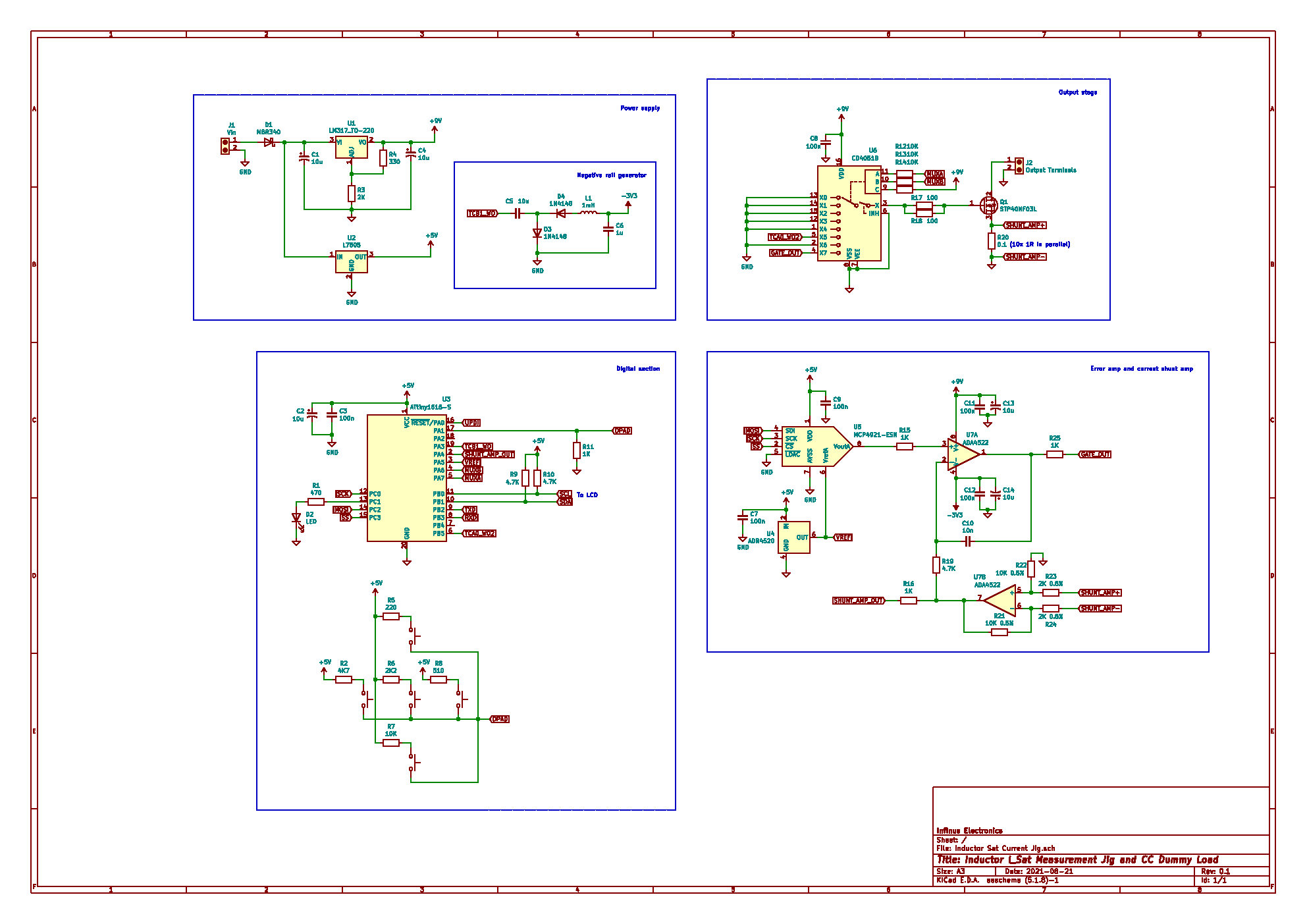
Click here to download a higher resolution version.
Opamp choice
I decided to go with the ADA4522, a really nice – and expensive – low offset voltage opamp. There are probably cheaper opamps that would suffice, but the ADA4522 was all I had on hand. The low offset voltage is important here, since I plan to have mA level resolution with a 0.1Ω shunt, so sub millivolt input offset is kinda necessary.
The ADA4522 has a great noise spec, although I suspect with the janky perfboard construction much of that is going to go to waste.
Negative rail generator
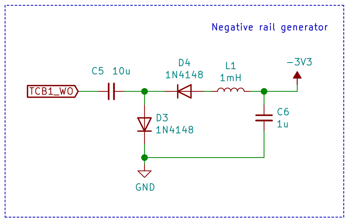
While the ADA4522 has rail-to-rail output capability, its not perfect. With no load, and 9V single supply, I measured the output to sit at a few tens of milivolts, not good enough.
So, I leveraged one of the PWM outputs of the microcontroller to implement a very crude charge pump inverter, which allowed the ADC to actually read 0 when there was no current flowing through the system.
L1 is there to try to provide more smoothing to the output voltage. With it and all the capacitors present, I achieved an 8mV peak to peak ripple with a switching frequency of about 100kHz, which didn’t result in too much noise at the output of the opamp.
With the negative rail present, the output of the opamp sits at 5uV with respect to ground, according to my Aneng AN8009 (great hobby level multimeter by the way). Of course, its a cheap multimeter, so take that figure with a huge grain of salt. But the key takeaway is that it is so small that I have no way of properly measuring it, which in my eyes, is an absolute win!
Differential current shunt amplifier
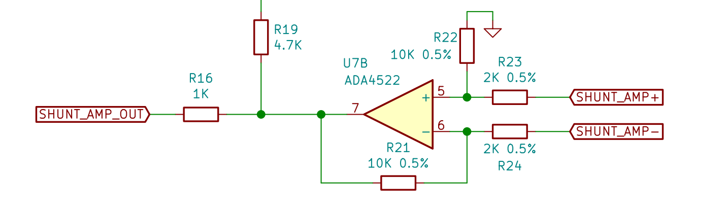
The four resistors R21 to R24 need to be as precise as possible, if not in terms of absolute tolerance, then at least in terms of their ratios, otherwise the accuracy of the differential amplifier really suffers. Normally 0.1% or better resistors would be specified, but the best that I had were 0.5% SMD thin film resistors, so I went with those.
Care must be taken to make the soldering operation of these precision resistors as quick as possible. Prolonged heating may cause the resistance of these parts to drift by an unacceptable degree. Usually the datasheets for these precision resistors specify a maximum time and temperature to which these parts should be exposed.
Using the parts shown, I was able to get a 5x gain differential amplifier that was accurate enough that none of my basic instruments were able to measure any error, so now basically, the main source of error is the tolerance of the current shunt itself.
Digital section
At the heart of this project is the ATTiny1616, which is part of the new tinyAVR series that supersedes the older ATTinies like the ATTiny44. These are a great departure from the old ATTinies, as their price point makes them actually worth going with compared to the ATMega line. They have great performance, rich peripherals, none of that USI rubbish (finally, no finicky I2C!), and I’m seriously in love with the new UPDI interface, no more fiddling around with using Arduinos as programmers; a USB to serial adapter, 1 diode, 1 resistor and off we go.
Speaking of new AVR micros, Microchip now also has a new line called the AVR DA and DB line. These are really awesome too compared to the old ATMegas. Basically, given their price point, no hobbyist should ever go with the ATMega328 ever again. These are just so much better, and cheaper too!
Be sure to check out megaTinyCore and DxCore . Bringing these microcontrollers into the Arduino ecosystem just makes them that much easier to whip quick and dirty projects like this one out in no time.
D-pad
Due to the pretty limited I/O pins available on this microcontroller (it is, after all, an ATTiny), I opted to use the classic resistor network trick to read the buttons, all via 1 I/O pin. I found that with the speed at which the program loop executed, debouncing wasn’t necessary, but your mileage may vary.
One downside of using an analog based approach like this is reading simultaneous button presses gets really finicky quickly. Fortunately, I wasn’t planning to implement any such functionality, so it was a non issue.
ADC oversampling and decimation
This microcontroller has two 10-bit ADCs built in, both with a really nice feature: accumulation. Basically, the ADC is able to continuously add conversions to previous ones, making oversampling much easier to implement. Using this technique, I was able to get a nice bump in resolution from 10 bits to 12 bits, not bad.
I should note right here that this oversampling and decimation technique is not magic, within a certain range, it really does work quite well, and can provide readings with satisfactory accuracy and noise performance; but the ADC is still only 10 bits.
Below a certain level, there just isn’t enough data available to reliably read the voltage anymore. I found that in my case, with my perfboard construction, this happened at about 50mV input to the ADC with a 2.048V external reference. The readings were just jumping all over the place, and accuracy was pretty poor. In the single digit millivolts, it was just completely off.
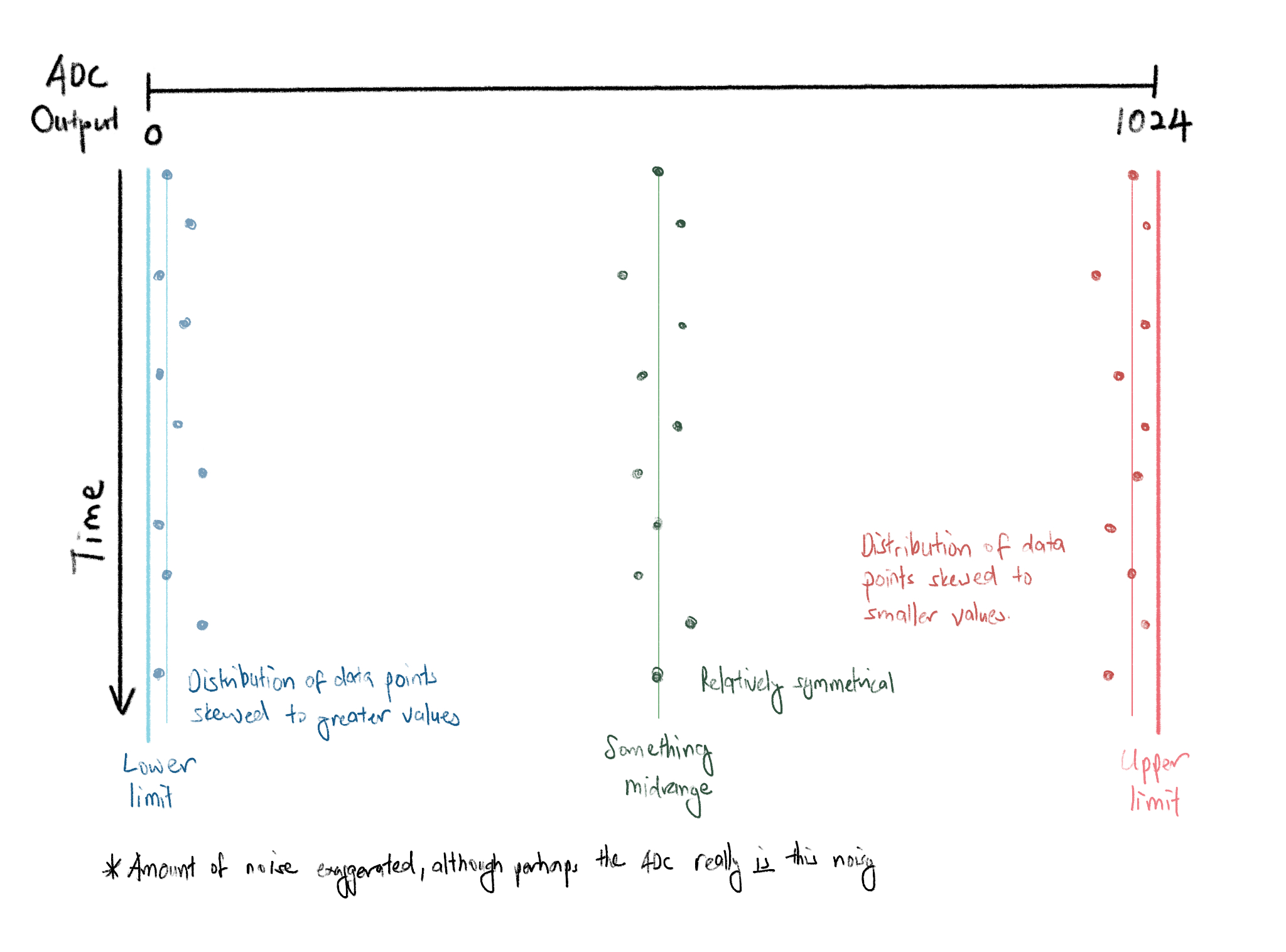
The reason for this is that oversampling and decimation is essentially a statistical technique, and assumes that, with the noise inherent to the system, the ADC readings will fluctuate about a median value with a symmetrical distribution. In the middle of the ADC’s range, that is exactly what happens, and thus this technique works quite well.
However, when it comes to the extremes of the range, such a symmetrical distribution simply isn’t possible, since the ADC can’t read negative voltages or voltages above VREF. With proper low noise layout, one could probably squeeze out a little more performance from the internal ADC, lowering that 50mV figure, but I suspect that the law of diminishing returns would set in rather quickly.
SPICE-ing the analog section
SPICE is just one of those things that really intimidated me for whatever reason. As a hobbyist, I just never really tried it at all.
I was going to take the super simple approach that Dave from EEVBlog took, until I stumbled upon [that blog post], which showed that the LM324, which in my eyes is the beginner op amp, oscillated like crazy without some sort of compensation. With all the frustration going on in the SMPS Chronicles Boost Converter project, I really wasn’t in the mood to solder up yet another circuit only to have it exhibit critical flaws.
So, I bit the bullet and gave LTSpice a go. And boy oh boy was I glad I did. The ADA4522 opamp also oscillated without compensation, at least in the simulation, and I could not imagine the dread if I were to build it up and it did the same in real life. I also modeled in the parasitics of the CD4051 (to the best of my abilities), just in case.
It is at this point that I should make it clear that I have absolutely no idea what I’m doing when it comes to SPICE. I’m sharing this section to hopefully show you that SPICE is really not as intimidating as many hobbyists, myself included, and it can really save you a lot of headaches and wasted components.
Barebones circuit
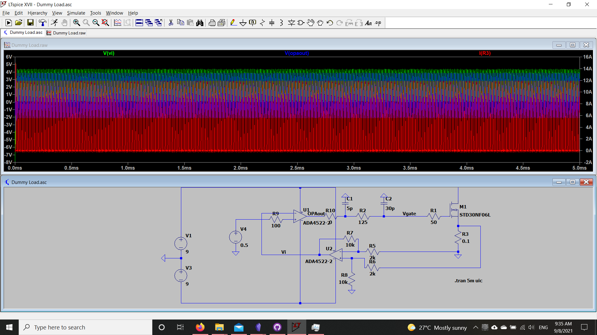
First, here is the simplest possible circuit, with everything just directly connected to each other. Note how the the output is just completely unstable and is basically oscillating rail to rail.
The first two things that I tried were:
- Adding a resistor at the output of the ADA4522 to try to isolate the parasitic capacitances of the MOSFET gate and the MUX
- Adding a resistor between the output of the shunt amplifier and the non-inverting input of the error amp
No luck in both cases.
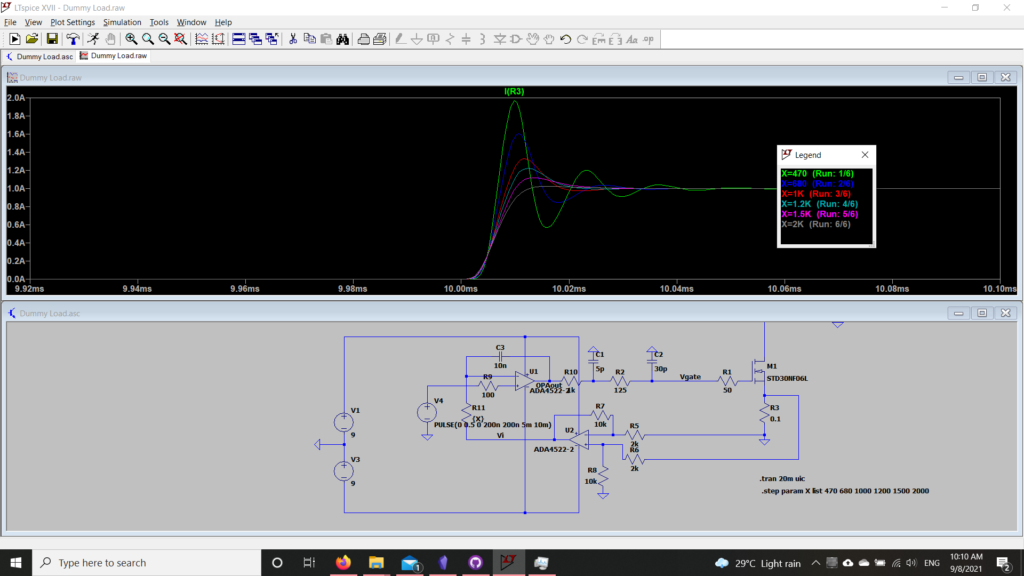
Adding the compensation network
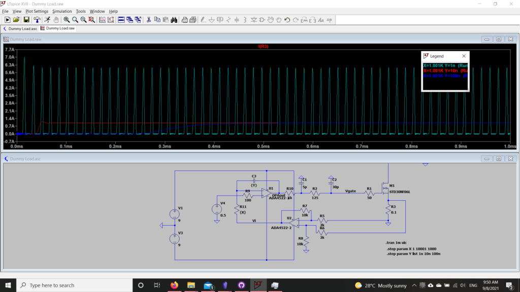
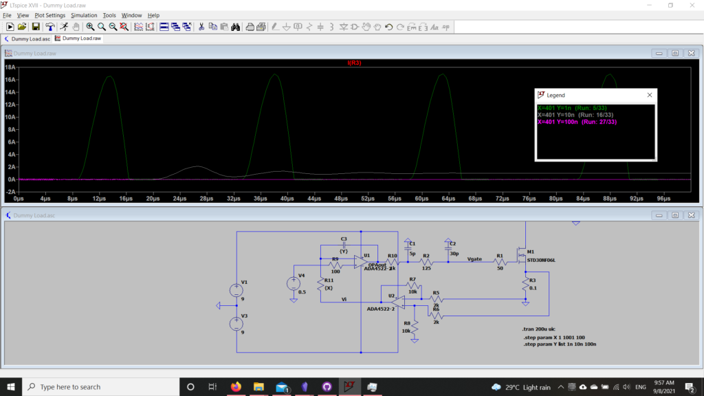
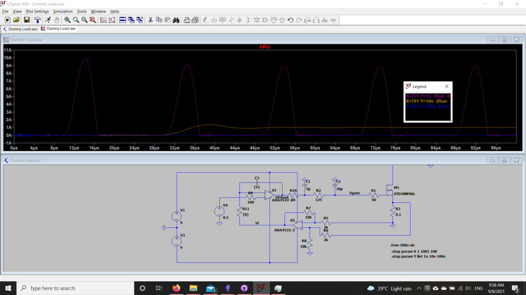
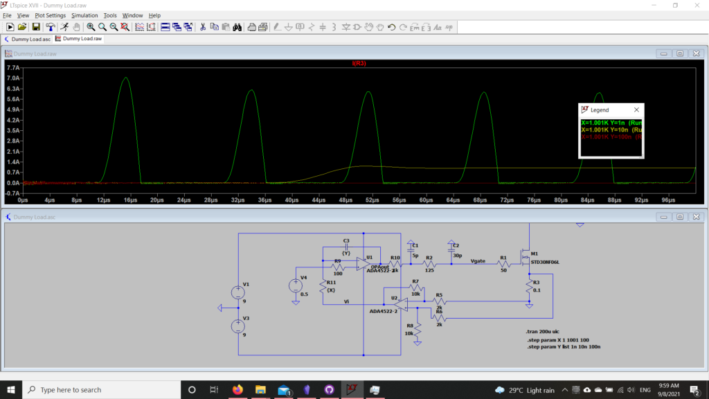
Finally, as suggested in this blog post I added in a type 1 compensation network, consisting of C10 and R19. Using the STEP command, I got LTSpice to try a whole bunch of values to see which ones were going to stop the oscillation most effectively.
I have to say, I was surprised by the results. Most of the combinations I specified almost completely eliminated the oscillations.
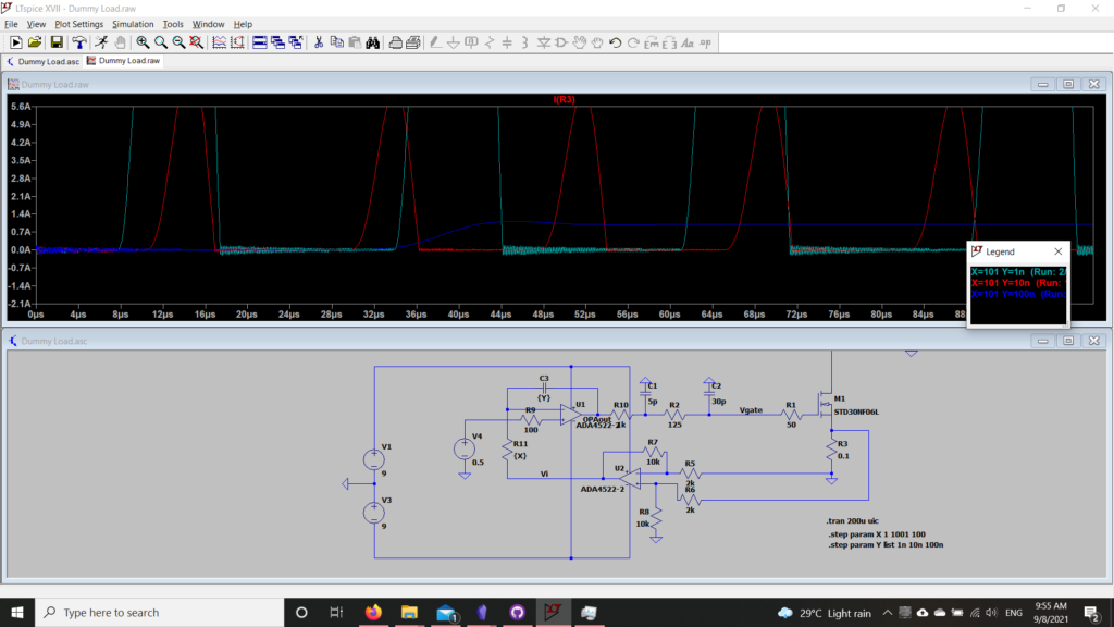
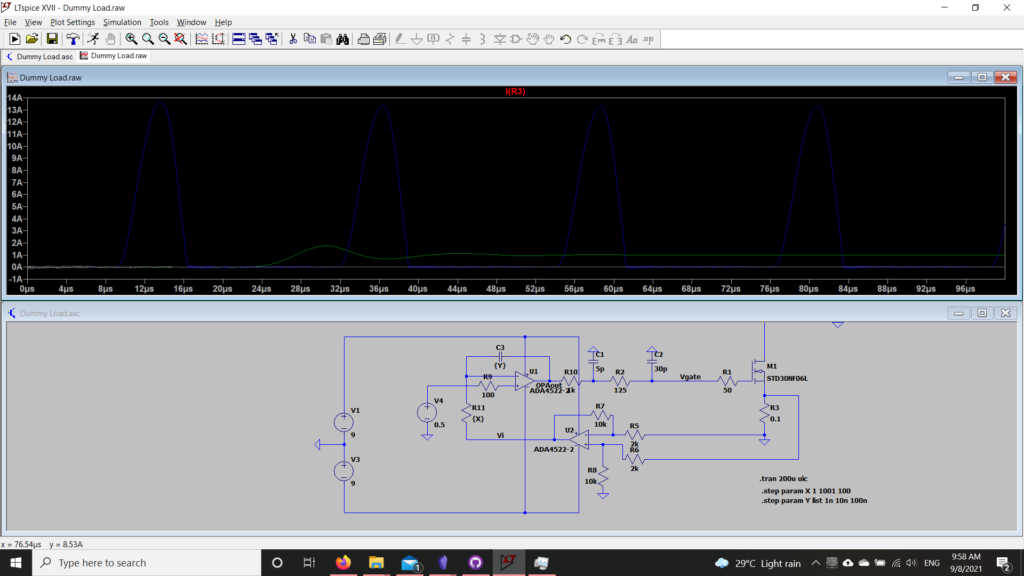
It was then just a matter of trial and error to get the best step response out of the circuit. I settled on a combination of 10nF for C10 and 4.7kΩ for R19. In bench testing the completed unit, none of the input voltage and set current combinations that I tried resulted in any oscillations at the gate of the MOSFET, so I guess the SPICE-ing really paid off.
Trying to get rid of the oscillations
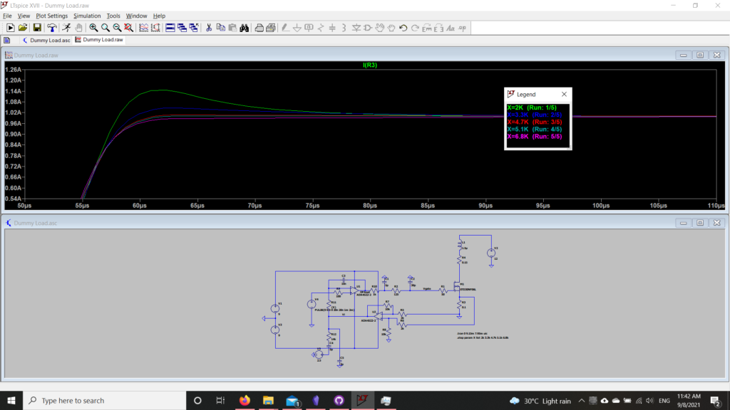
Taming the turn on transient response
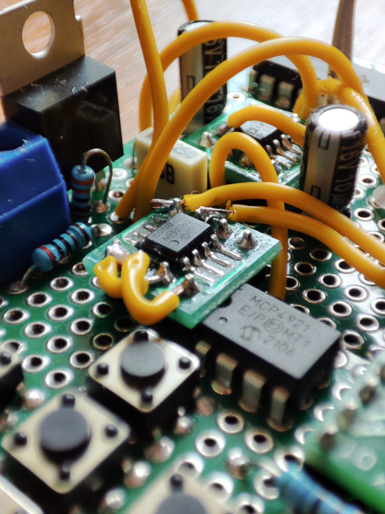
Construction
Grounding
Because this is a mixed signal circuit, to keep noise down, separating the analog and digital ground return paths is generally called for as far as I understand. It is quite difficult to achieve this on a perfboard, but do try your best. The concept of separate return paths can be really confusing – it certainly was for me – but I find that thinking of it like this really helps:
Wires aren’t perfect, they have parasitic resistances, capacitances and inductances. Just for the sake of simplicity, we are only going to focus on the resistances, it should make the point really clear. Just note that adding in the inductance and capacitance parts only makes thing worse.
When digital pins switch states, they require a sudden gulp of current to charge up any capacitances. Picture these two scenarios when this occurs:
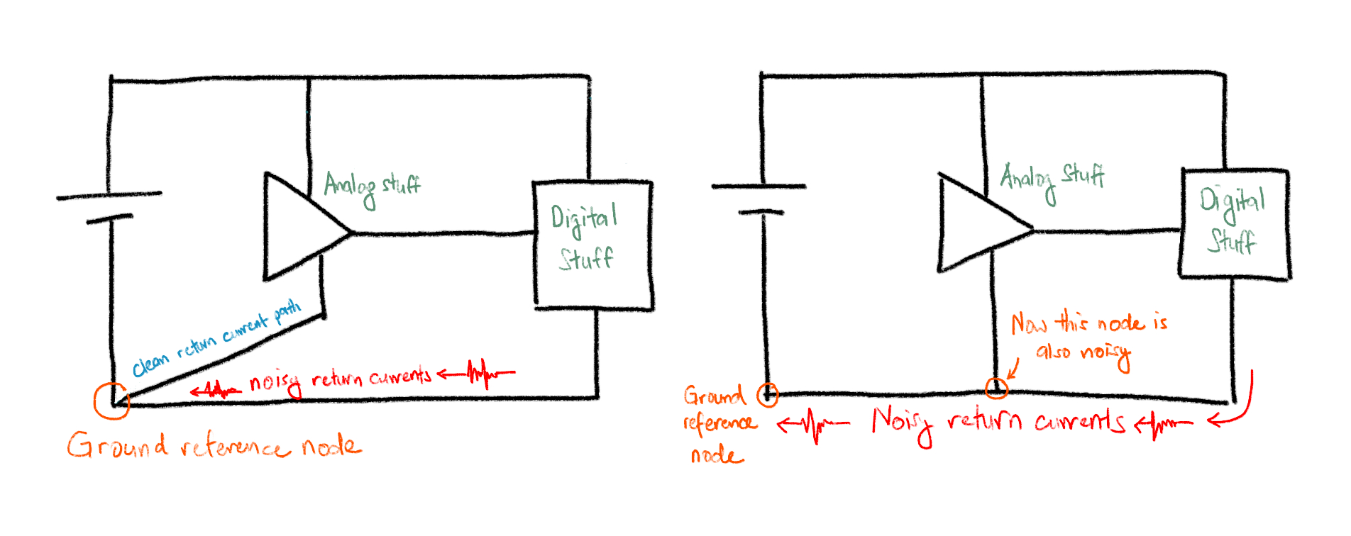
In the left approach (known as a star ground), everything has its own, proper return path, so we’re all good.
The same cannot be said for the approach on the right, however. When the processor draws that sudden gulp of current, the parasitic resistance causes a sudden shift in the potential of the “ground” node seen by the opamp. This change in potential gets coupled in to the sensitive analog circuitry, and manifests as noise.
When accuracy is required, thinking carefully about all the return paths becomes even more important, different “ground” nodes on a board could very well be at different potentials; it is important to ensure that all the stuff responsible for measuring voltages have their ground reference potentials as close to each other as possible. Often, this means actually connecting them to the same point, ie star grounding.
Just to drive the point home, I chose the output terminal’s ground to be my ground reference. Just by the small amount that this circuit draws to operate, the ground of the input terminal sits at a jolly half a millivolt-ish above the ground reference.
Remember that for 1mA, the shunt only produces 100uV of potential difference. Thus if you were to measure the voltage across the current shunt, but used that input terminal as a reference, straight off the bat you’ll have an error of 5mA. And we’re only dealing with 12-bit resolution here (4096 count). Imagine how difficult it is to control this issue in say, a 6.5 digit multimeter, which has a 24-bit or better (more than 16 million count) ADC.
In this instance, the use of the differential amp to amplify the current shunt is meant to improve the accuracy by directly amplifying the potential difference directly across the terminals of the shunt, which are the nodes most sensitive to small differences in potential in the entire circuit.
All that’s left to do is to make sure that the DAC, ADC, and opamp are all referencing off the same ground potential, and the accuracy should be more than good enough for 12-bit resolution. The path which the large dummy load currents flow through is largely eliminated from the equation, which is great as it has the highest chance of producing unexpected voltage drops.
Decoupling
As mentioned above, when digital pins switch, they draw a sudden gulp of current, which introduces noise. So, decoupling caps are necessary on all IC’s in the circuit; for the digital IC’s they provide a reservoir of energy when such switching events occur, and for the analog IC’s they smooth out these spikes (to some degree) before they enter the power pins.
If you’re using through hole ceramic capacitors, solder them as close to the power pins of the IC’s as possible to keep parasitic inductances to a minimum. I prefer to use SMD 0805 ceramic capacitors directly tacked on to the IC pins, as they are as low inductance as one can get for perfboard construction, and 0805 fits really well between adjacent holes on a perfboard.
Inductances slow down the delivery of current to the IC’s, thus they directly reduce the effectiveness of decoupling capacitors. So, it is rather important to reduce them as much as possible.
Soldering sensitive components
Like I mentioned above, try your best to take as short a time as possible when soldering precision parts, as heating will cause them to drift. Check the datasheet to see what is permissible.
Measurement: a lesson in loop area
Because this is intended to be used to test power supplies, mains earth referencing can be a big issue. Make sure that you are cognizant of which nodes are referenced to where, so that you don’t blow up your oscilloscope.
Also, trying to measure the output noise of the differential amplifier proved to be a pretty interesting challenge in and of itself. Using the conventional ground clip on the scope was fine, using a small isolated wall wart to power the circuit.
That is, until I turned on the ATX power supply I was using as a load. Huge noise spikes appeared. It kinda puzzled me for quite a while, as I tried to figure out why the circuit was letting so much high frequency crap through.
Until I remembered about low inductance grounding. The moment I swapped out the ground clip for one of those slip on ground pin things, the spikes instantly vanished. Just goes to show how tricky measuring noise can be, and if you weren’t aware of lead inductance issues, then well, you could really come a gutsa.
Anyway grounding issues aside, I managed to get this load to dissipate 40W continuously with a modest heatsink and a small fan. Certainly good enough for my needs. As for the saturation current measurements, this does its job really well too, although all the fast switching of much greater currents injects a tonne of noise into everything.
The code
In essence, the code is a state machine, with one state for each mode. It really is quite basic, so I won’t dive into too many details here.
One thing to note if you want to follow along: set the millis() source to RTC before uploading the code. TCA0 is used to generate the PWM output for the inductor testing functionality.
Check out megaTinyCore and DxCore , the setup code for the PWM generation with TCA0 and ADC Oversampling is adapted from there as well.
If you’d like to mess around with the registers, and would like to work with bitmasks to keep everything readable (instead of just a bunch of 1’s at random bit positions), you should check io****.h for those definitions. So, for example, in my case with the ATTiny1616, all the bitmasks are defined in io1616.h. These are located in the megaTinyCore folder in your Arduino cores folder, which in turn is located in Appdata Local, not Program files.
Check out the code here .
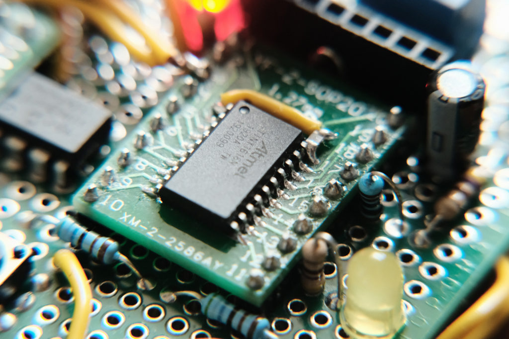
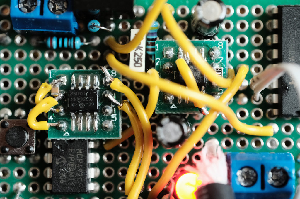
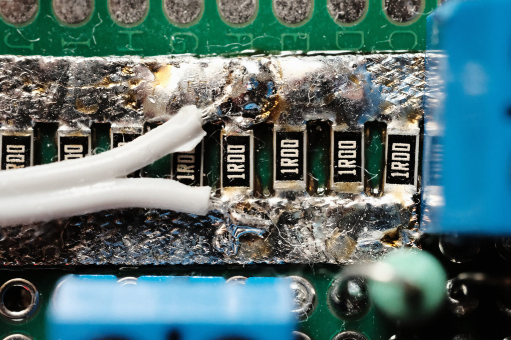
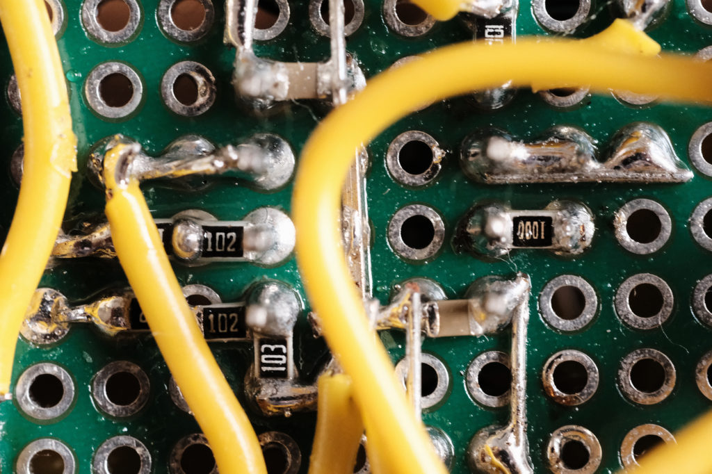
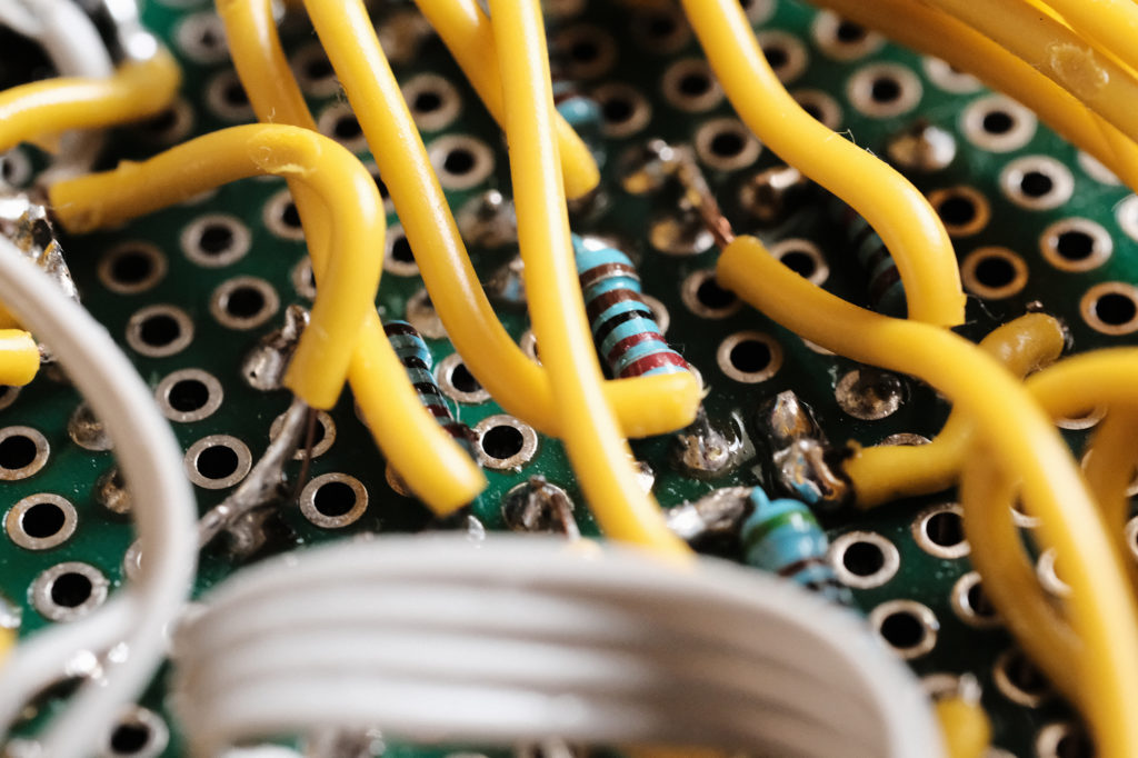
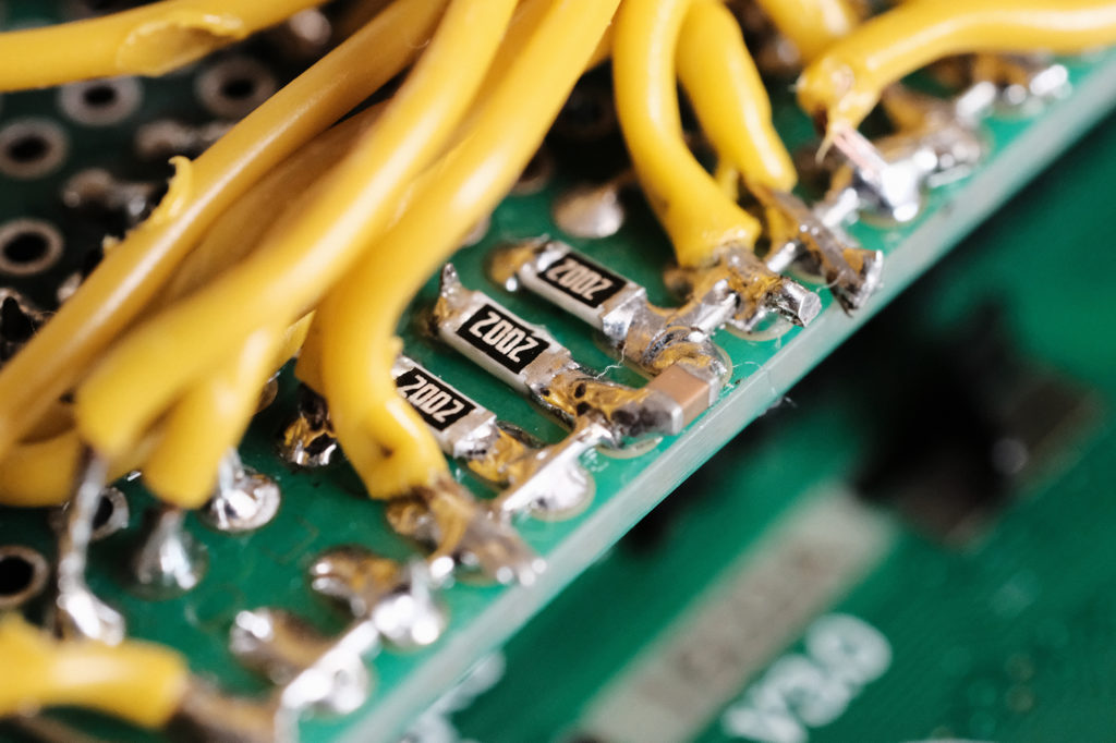
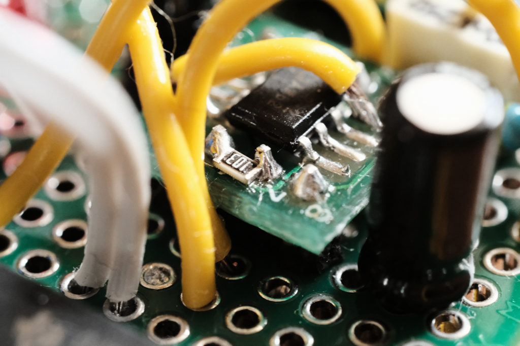
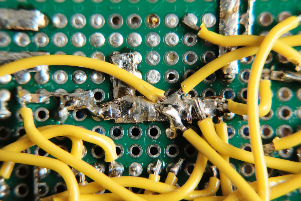
Gallery
As always, here is some eye candy.