Before reading on, please refer to the previous part/MK1 of this project, otherwise some of the stuff here might seem a little odd.
Schematic
Check out the design files here
Compared to the MK1 design, the gain stage is essentially identical. The differences are just the addition of an analog switch to control the AC/DC coupling selection and the inclusion of an additional ESD/EOS protection TVS diode.
The analog switch was necessary because I wanted to squeeze everything in a 30mmx20mmx7mm shielding can I found off Mouser, and unfortunately there were no electromechanical relays that would fit, at least not for an affordable price.
Testing its performance
Probe compensation/input capacitance
With the addition of the ESDSLC5V0LB ESD protection TVS diode, which claimed to have a maximum capacitance of 0.35pF, and the TS12A4516 analog switch having 5.5pF of input capacitance when off on each terminal, probe compensation was just barely possible.
One huge problem which made using this version of the front end really annoying was that the capacitance of the switch channel (to ground) is 16pF when it was on, i.e., it isn’t 5.5pF+5.5pF. This meant that every time I switched between AC coupling and DC coupling mode, the input capacitance would change and the probe would have to be recompensated.
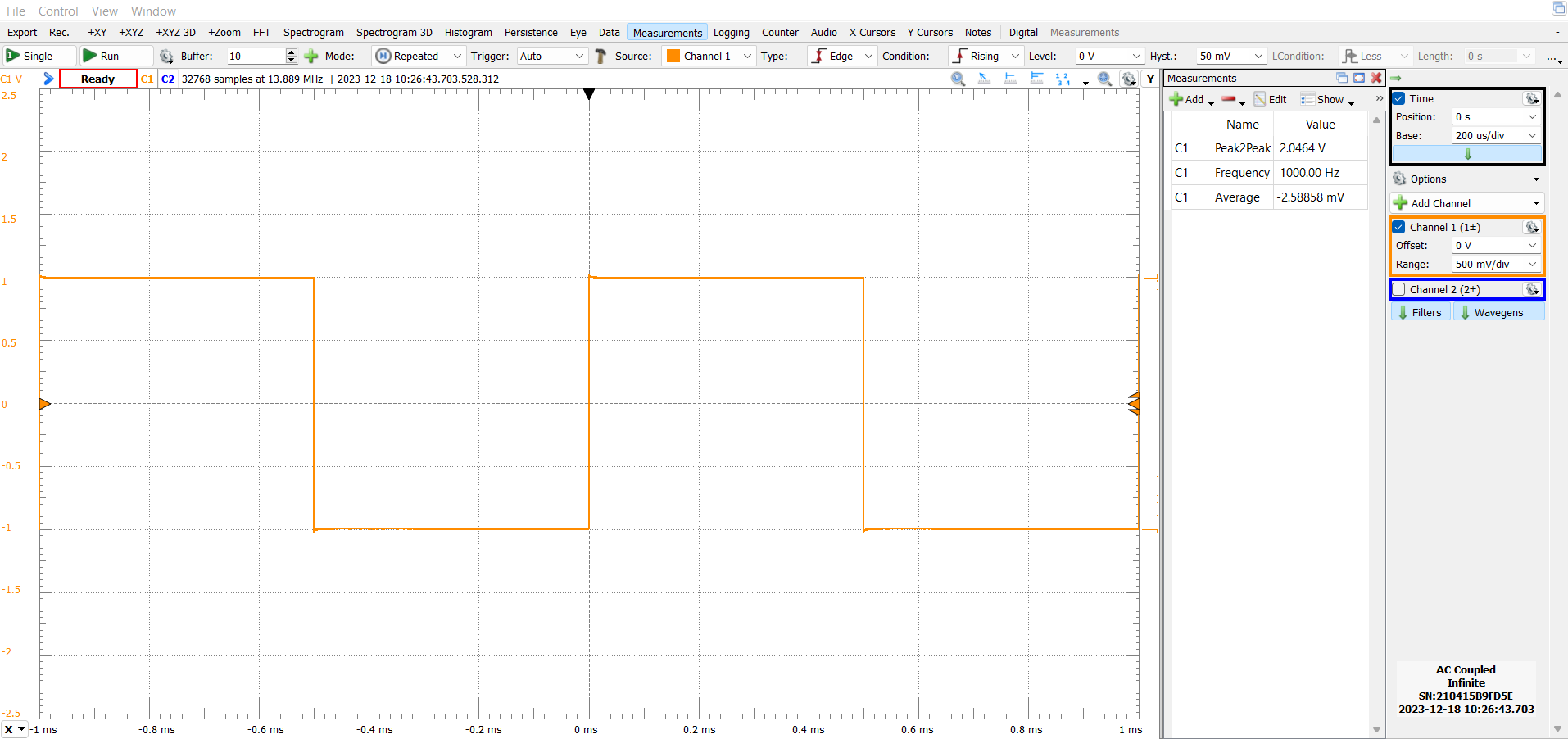
Compensated probe response, AC coupled mode

Coupling changed to DC mode with probe compensation unadjusted
Noise and crosstalk
Compared to the MK1 front end, noise and crosstalk are significantly reduced. Looks like the shields really are non-negotiable.
MK2 front end channel crosstalk MK1 front end channel crosstalk
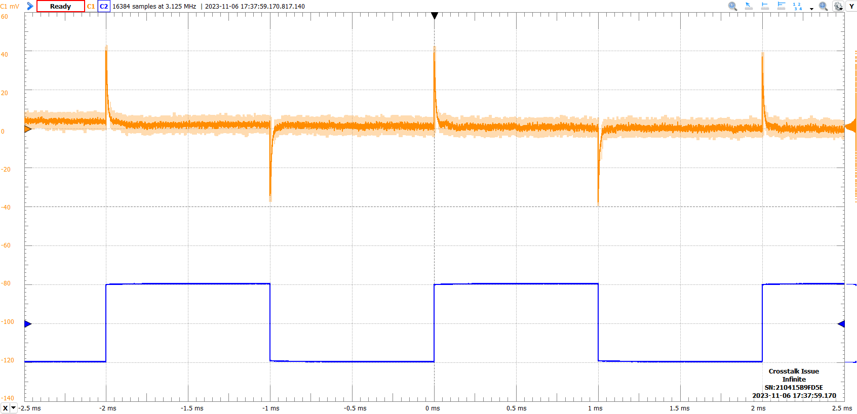
There’s just absolutely no comparison.
Also, I should also mention that in the MK2 PCB, I added a lot of GND stitching vias, which may or may not have helped in the crosstalk issue.
Noise pickup is a little harder to demonstrate objectively, but from playing around with the 2 front ends, aka waving my hand near them, the shielded MK2 is basically totally immune, while the unshielded MK1 picks up all sorts of stuff, sometimes with quite a huge amplitude too if my hand is within an inch or so of the high impedance input path.
DC offset in AC coupled mode
Something weird happens when the front end is in AC coupled mode, and the signal being fed in is some mixture of AC+DC. To illustrate the problem, take a look at the 2 following 0.1Vpk sine waves, one centered around 3V and the other around -3V:
AC coupled mode, input signal has -3V DC offset AC coupled mode, input signal has 3V DC offset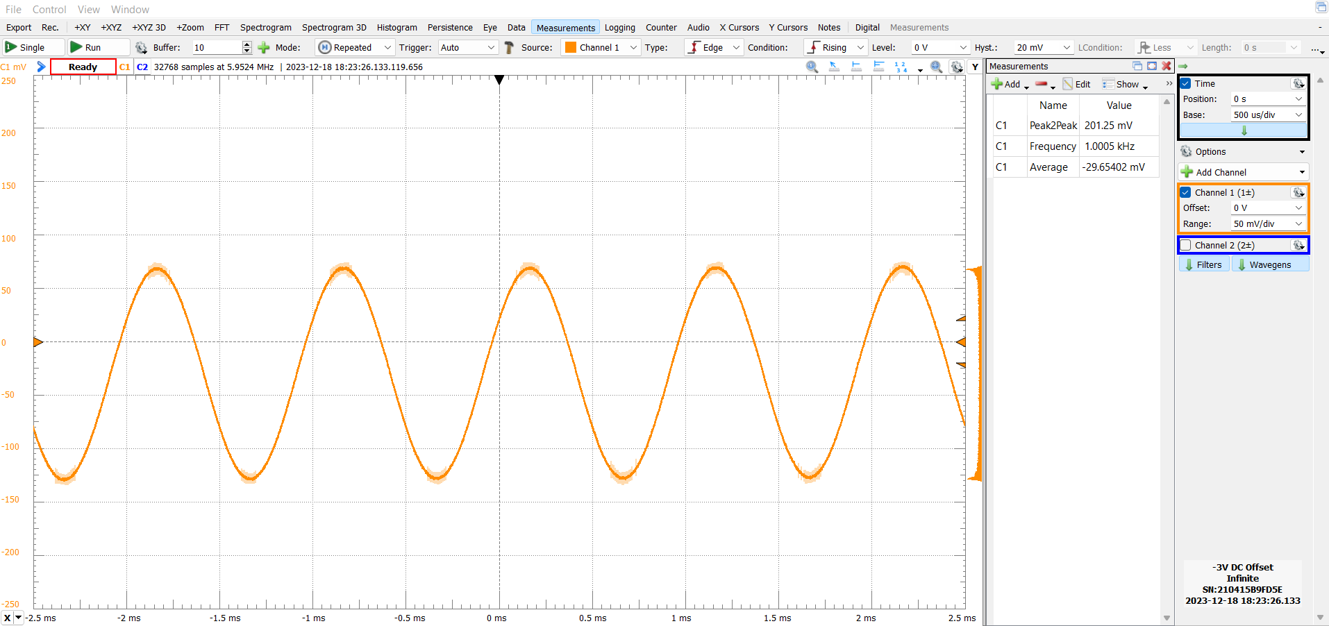
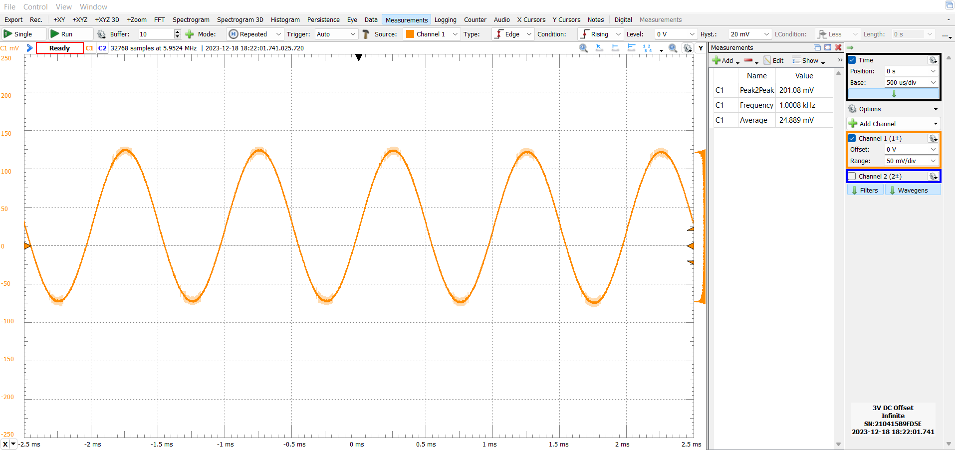
Even without resorting to the measurements, just by looking at these 2 waveforms, it’s immediately clear that something is not right. We’d expect both waveforms to be basically identical, but clearly, there’s some correlation between the output DC offset and the input DC offset.
I tried really hard to think of why this is happening, and to somehow validate my hypotheses. Was the analog switch somehow leaking current despite being off? Well, the datasheet specifies a typical leakage of 10nA maximum for a 9V potential difference between the switch terminals, which cannot account for the variation that we see here.
Could it be that some internal EOS/ESD protection diodes are somehow reverse leaking? Maybe, but this shouldn’t result in the variation that we see here; the offset should be constant.
Even more confusingly, when I heated the board up, this offset voltage basically went completely off the charts. Even holding my finger above the high impedance section (with the shield off but the frame of the shield still soldered on) causes quite a large change in this offset voltage.
So yeah, I’m completely stumped. All I know is that for the next iteration I’m going to ditch this TS12A4516 and replace it with an optical solid state relay, which should hopefully fix this issue.
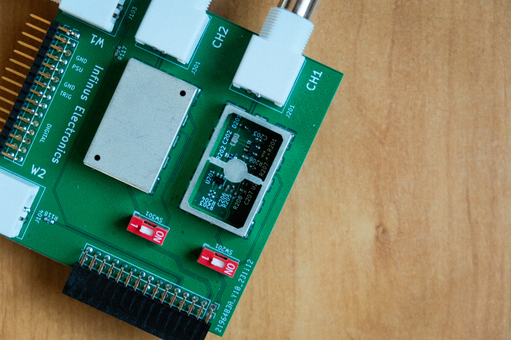
Completed board
Completed front end, together with shields Under the hood of one of the shields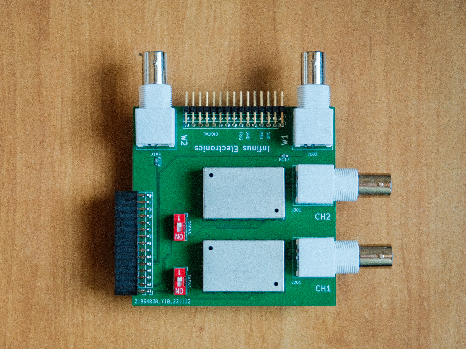
Conclusion
This revision was definitely a huge improvement over the MK1 front end. If I were very conscious of the issues outlined here, it would work for the vast majority of my use cases. However, I’m still not satisfied because a couple of its issues make it really annoying/unusable:
- Needing to recompensate when switching between AC and DC coupling
- Not being able to measure stuff above ±2.5V
As I write this, a MK3 is already in the works which would hopefully address these issues, so do look out for that.
Until then, thanks for reading!