The Analog Discovery 3 is a great debugging tool, but as I discovered here in a note on using it with 10x scope probes, the input capacitance was too high for the probes to be compensated correctly.
Custom LNA design
To combat this, I decided to design an amplifier that would have a low input capacitance so that we fall within the 5-35pF compensation which is typical of these 10x scope probes.
As an added bonus, because the Analog Discovery 3 cannot provide enough gain to get a nice signal after a 10x scope probe, the LNA can also add a gain of 10.
This should mean that no performance is sacrificed when using 10x scope probes, which is great since 10x scope probes load down the circuit under test a lot less, which comes in handy when measring oscillators etc, as I found out in one of our labs at Cambridge.
This is essentially a 2 stage amplifier, implemented with the OPA356 CMOS opamp with a GBWP of 200MHz. The first stage gains the signal up by 5, and the second stage is a unity gain inverter, giving a total gain of 10x when driving the ADC on the Analog Discovery 3 differentially. This compensates for the 10x probe attenuation.
Since the OPA356 is a CMOS opamp, the 1M resistor, R102, sets the input impedance to a nice, well known value that the probe is specified to work with.
R108 and R114 isolate the outputs of the opamp from the capcitance in the rest of the signal path downstream.
Check out the full schematic here .
Opamp selection
Bandwidth requirements
The number 1 constrain on this design is that I don’t want this amplifier to constrain the bandwidth of the Analog Discovery 3 any further.
On the product page for the Discovery BNC board , the claimed system bandwidth of the combination of this BNC input board and the Analog Discovery 3 is 30MHz.
Therefore, with a gain of 10, the opamp needs a gain bandwidth product of at least 300MHz, and preferably much higher.
Not only that, the opamp has to be able to output the signal at 30MHz, i.e. the large signal bandwidth of the opamp has to also meet this spec.
You can think of the large singal bandwidth as the speed the output stage of the opamp can drive the output to levels in the volts peak-to-peak range, as opposed to the small signal bandwidth and the gain bandwidth product specs, which are usually measured (at least for the TI parts I considered) when the output swing is approximately 20mV.
One example of something that would work is the OPA817, with a nice gain bandwidth product of 400MHz, and a large signal bandwidth of 250MHz driving 2V peak-to-peak. It also has a nice wide supply voltage range, up to ±6.3V.
It also costs more than £8 per chip on Mouser in single quantities…
Turns out that it is really not trivial to find an opamp that would do this and still be relatively cheap.
Hence, I chose to split the gain into 2 stages, so that a relatively cheap OPA356 can be used (about £2.50 per opamp), which would still be cheaper than using the single OPA817.
Max supply voltage and output range
The common mode input range of the Analog Discovery 3 is ±2.5V only anyways, so the low voltage OPA356 should do just fine being powered at ±2.5V by the Analog Discovery 3’s bipolar supplies, with a couple LDO’s of course to prevent accidental setting of the supplies to something like ±5V from immediately releasing the magic smoke.
This also means that we don’t lose the supply functionalty, as any voltage above 3V ish should give the LDO’s plenty of headroom to work with, meaning to say that we can still use the adjustable power supplies on the Analog Discovery 3, albeit at a reduced range.
Single ended input to differential output
One more quirk of the Discovery BNC board is that the negative input of the ADC is tied to ground, so straight off the bat we’re throwing away one bit of resolution.
Driving the ADC’s differentially should allow us to recover this lost bit, while reducing the required voltage swing by half, allowing the use of low voltage parts, perfect!
Of course, with 2 opamps driving the ADC differentially, offset voltage might become a problem. The OPA356’s offset voltage spec isn’t too bad, but offset voltage should be easily nulled in software anyway.
The main goal here, is ultimately still to get good signal integrity with a 10x probe.
Bandwidth simulation
Unfortunately I couldn’t figure out a good way to export a clean drawing from OrCad Schematic Capture PSpice
I used this simple project as an excuse to try out PSpice for TI. Still can’t believe that we can get access to Cadence software for free!
Just as a preliminary test, here is the bandwidth of just the circuit alone, with 22Ω output isolation resistors and a simulated output load of 1MΩ in parallel with 30pF single ended.
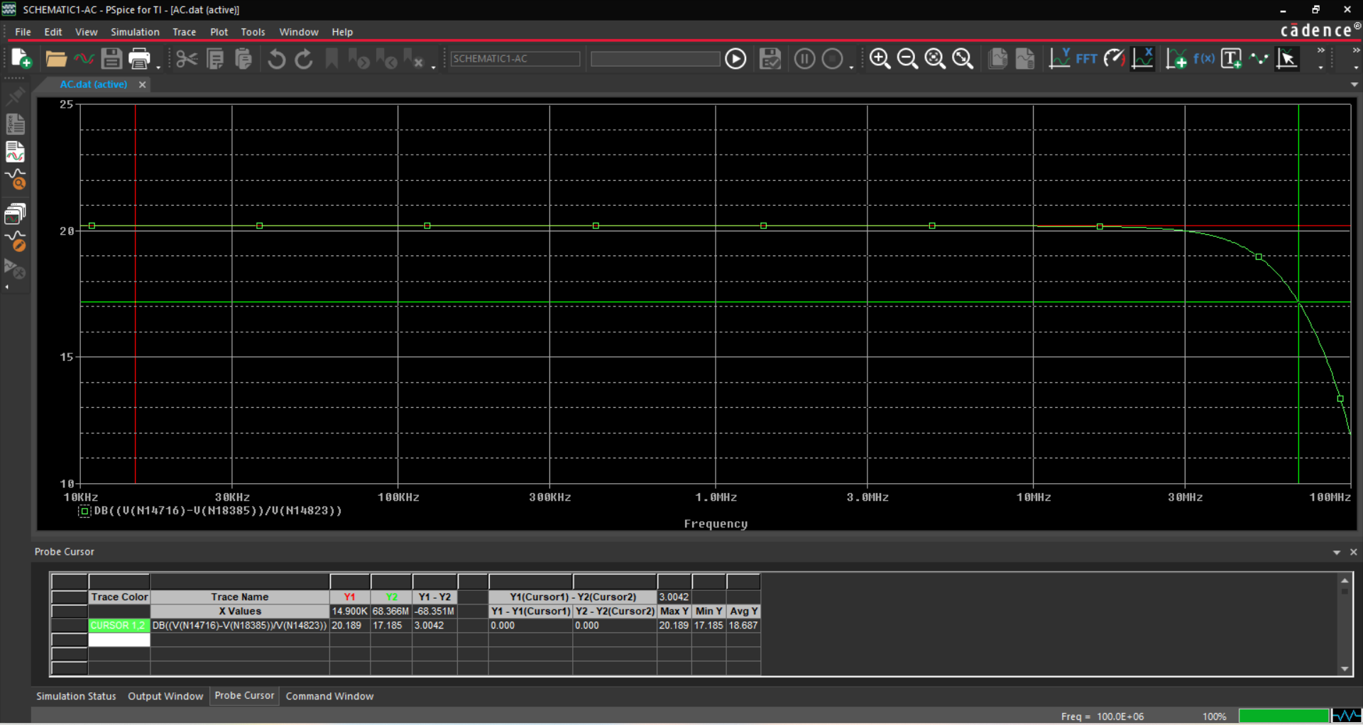
Basic PSpice simulation with 22Ω output isolation resistors
Immediately, the frequency response looks very nice, with almost 70MHz of bandwidth. Note that this is with a 4V peak-to-peak differetial output swing, so 2V peak-to-peak single ended, and the circuit has absolutely no problems hitting the 30MHz bandwidth target at all.
To investigate if the value of the output isolation resistors matter, here is a parameter sweep with 10Ω, 22Ω, 33Ω, 47Ω, 50Ω, and 68Ω at each output.
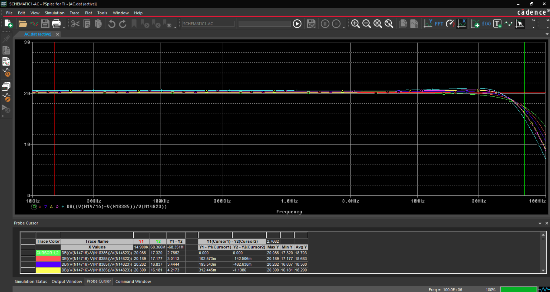
Parametric sweep of output isolation resistance
As expected, some curves are peakier than others, and the 3dB point does change slightly too. I found 22Ω to be a relatively good compromise.
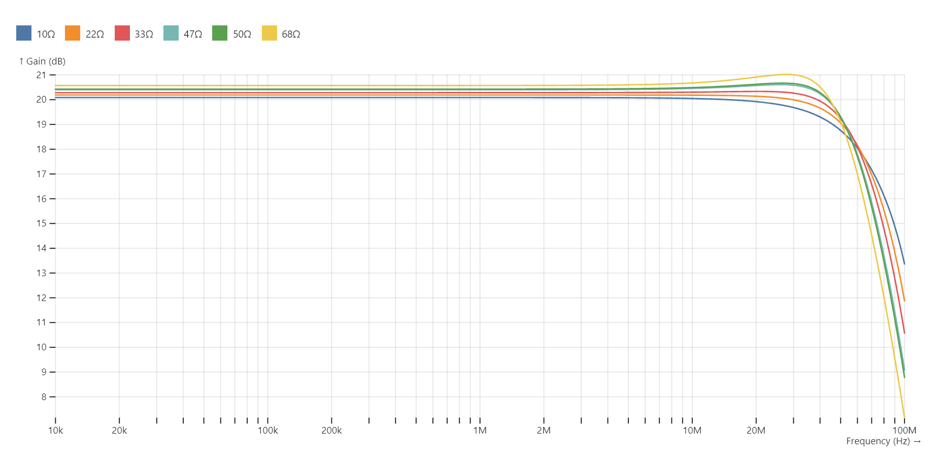
Comparison of different output isolation resistance values
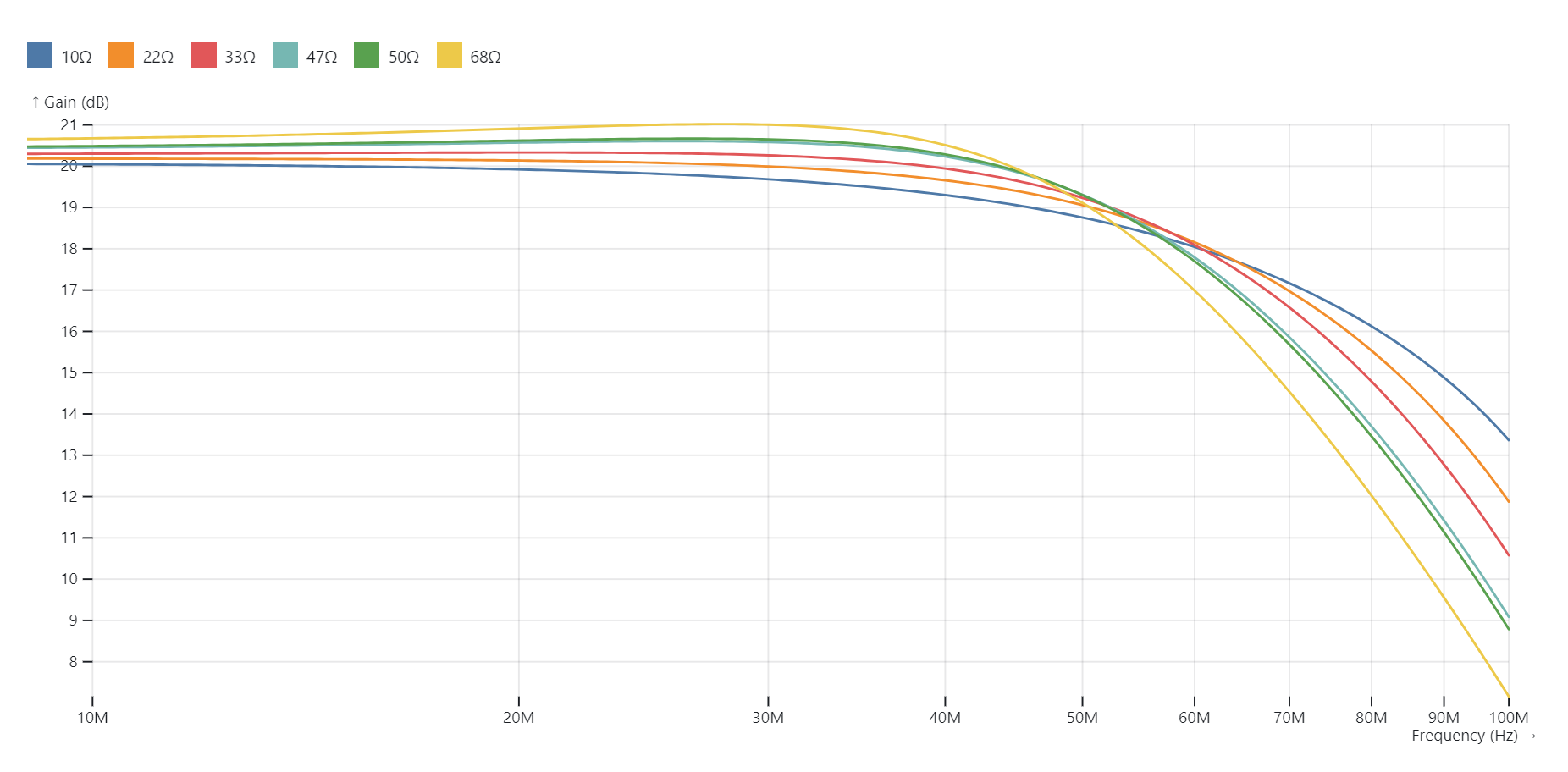
Zoomed in parametric sweep of output isolation resistance.
Completed board
I went with black soldermask because I thought it looks cool, and indeed it does!
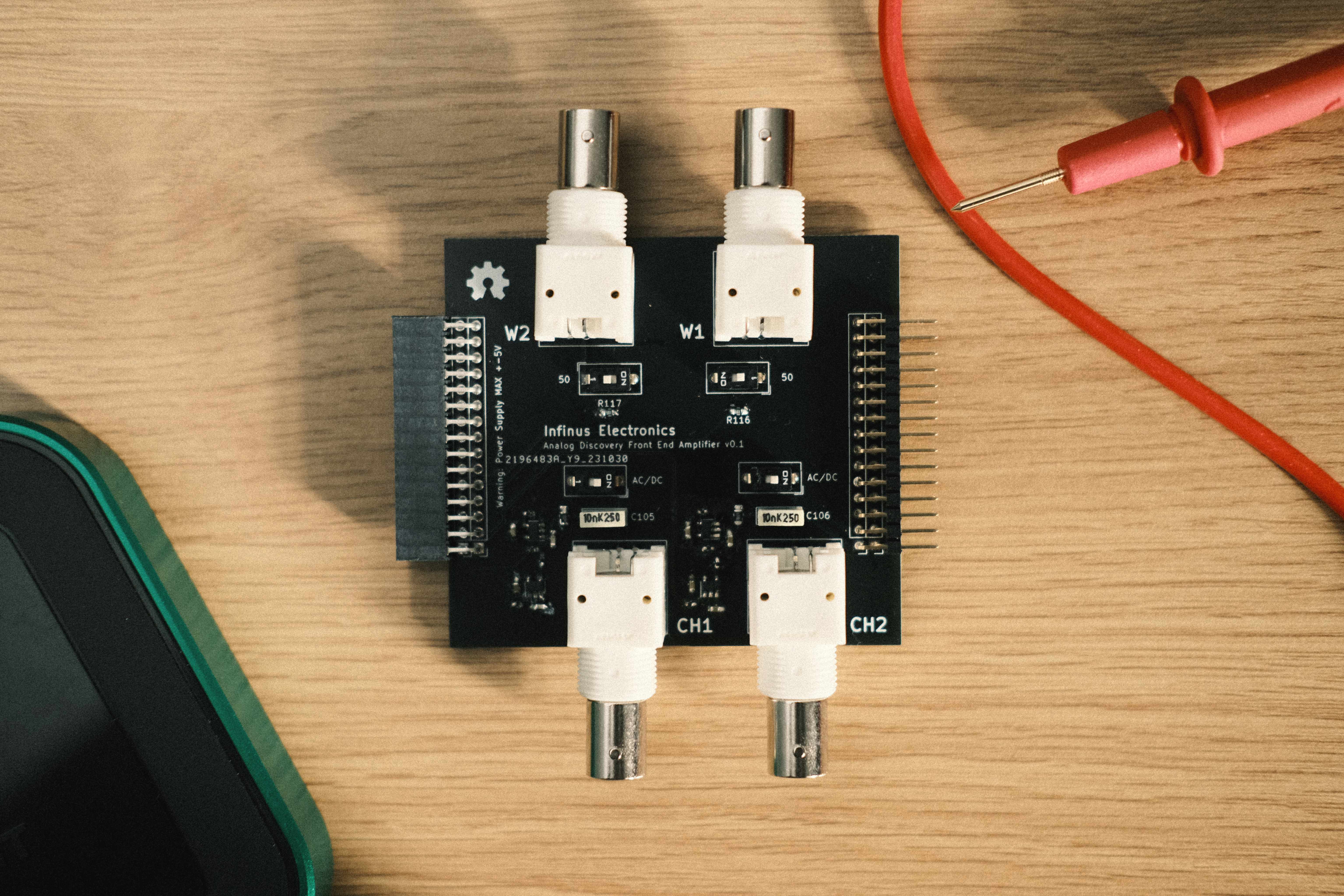
Completed build
Testing its performance
Input capacitance
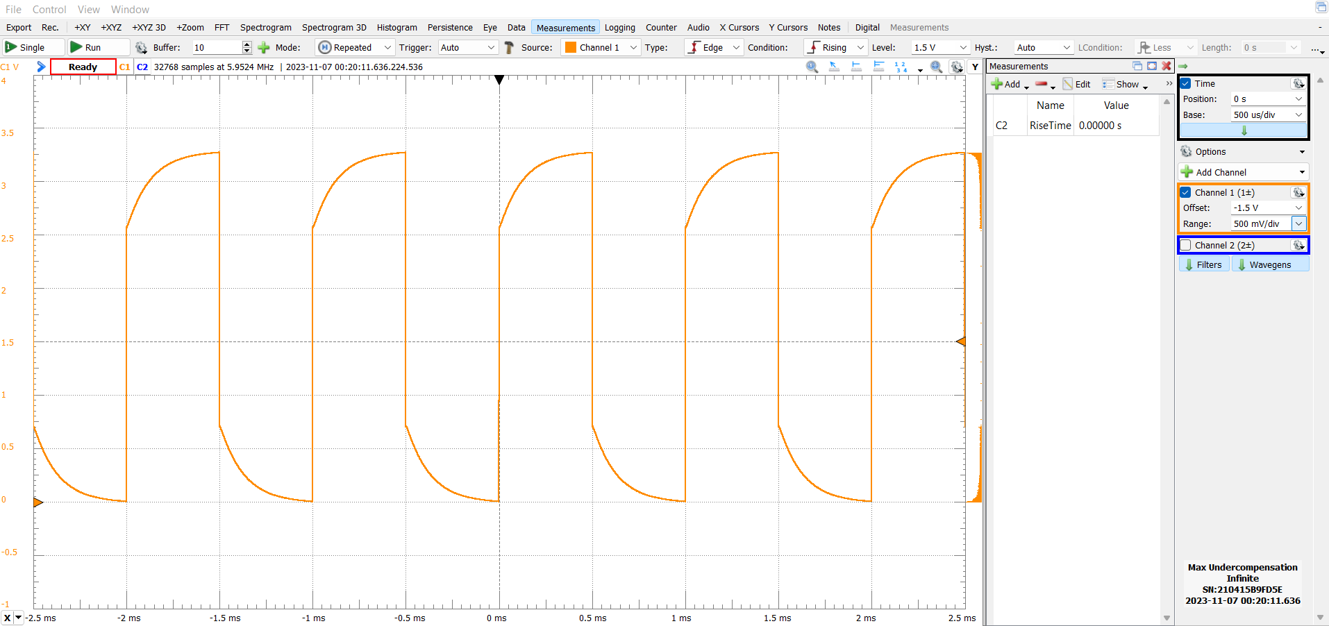
I guess this is the most important question of all: can I compensate my probes now?
Yes, yes I can.
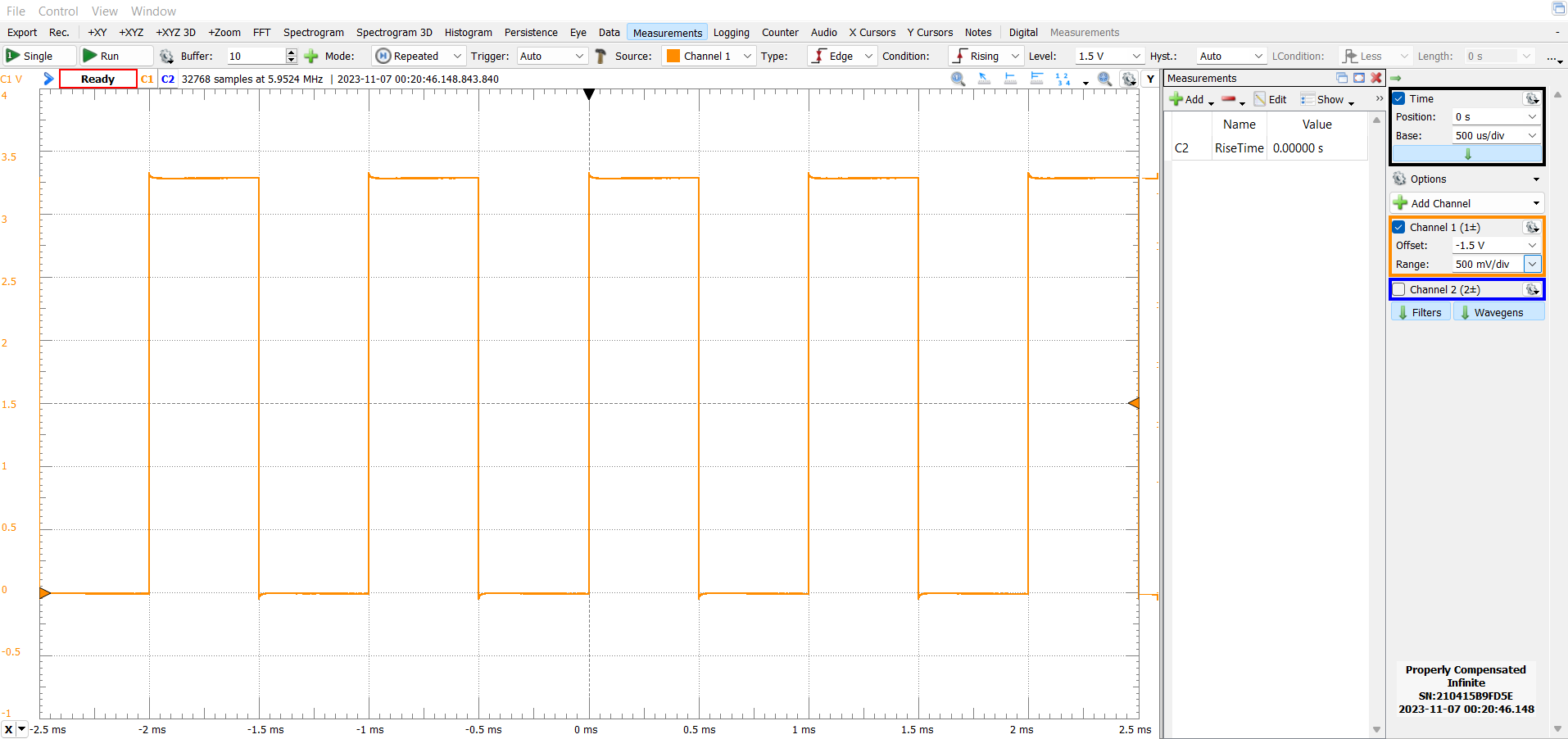
Proper compensation achieved!
And it’s well within the compensation range too:
This is at the far end of overcompensation This is at the far end of undercompensation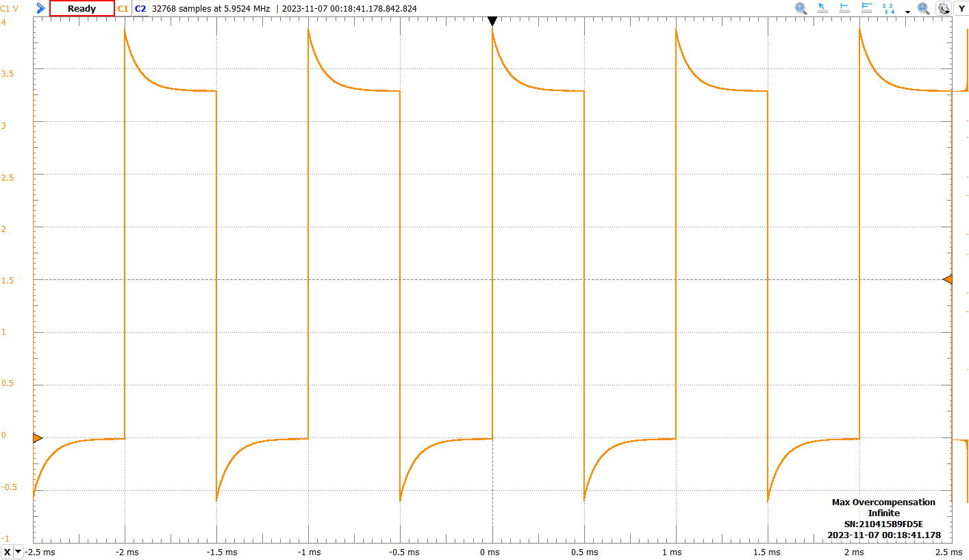
Bandwidth
Unfortunately, I don’t really have a good way to do a bode plot type measurement of the bandwidth, since the outputs terminate into 0.1 inch headers.
I’d probably try to measure it one day using the NanoVNA and some frankenstein-ed cables, but in the meantime, a good estimate would come from the rise time:
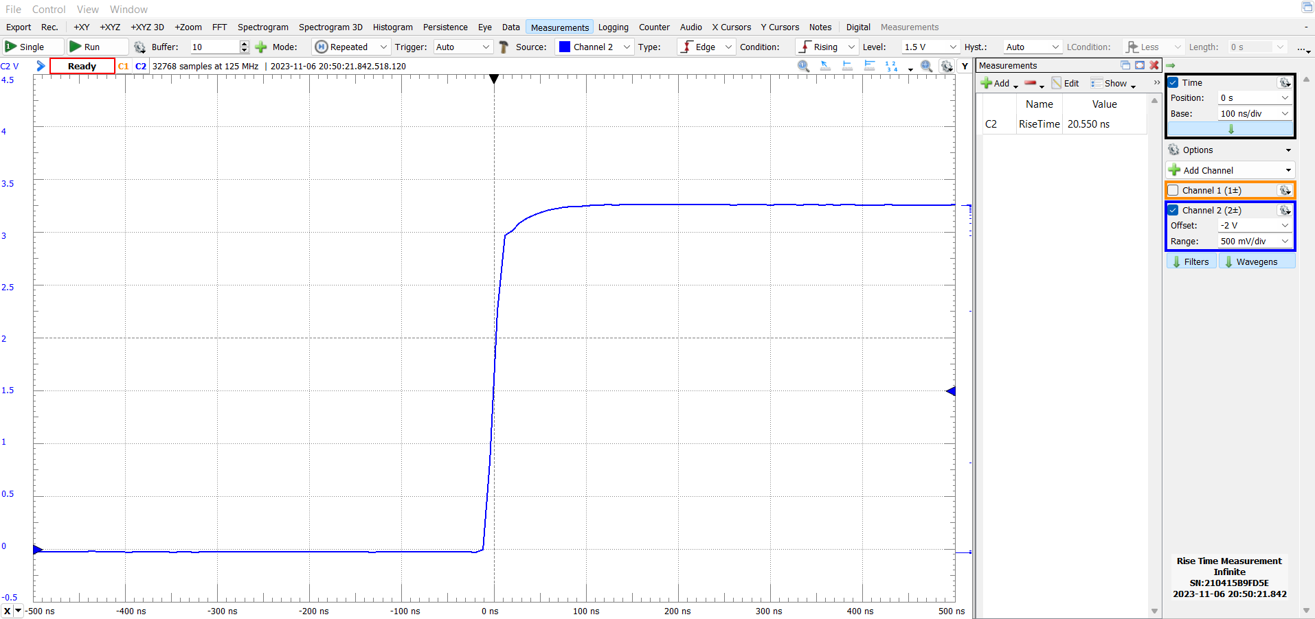
Approximately 20ns rise time
The Waveforms software reports that the rise time of the probe is about 20ns, assuming that the rise time of the digital outputs of the Analog Discovery 3 is much better than that, which it probably is.
Using the good old 0.35/rise time trick, I calculated the total system bandwidth, from probe to ADC, to be approximately 17.5MHz, as a quick and dirty project, I’m happy with that!
Also the edge literally only consists of 2 ADC samples when zoomed in all the way. So yeah, I think we can safely say that in terms of bandwidth, this LNA has absolutely no problem at all.
There aren’t any weird ringing issues either, just a tiny bit of overshoot, which I can definitely live with.
Output swing
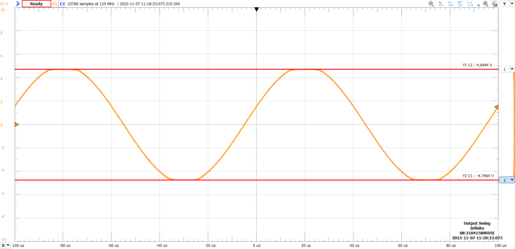
Output waveform with 5V sine wave being fed in to the 10x probe
The OPA356 datasheet claims that the outputs should be able to swing to within 100mV from the supply rails. With the ±2.5V power supply, nothing seems to be too egregiously wrong here.
Gain accuracy
I measured the gain (single ended input, differential output) to be 0.996 and 0.991 for channel 1 and channel 2 respectively. Good enough!
This error seems to be distributed across both the inverting and non-inverting channels.
Current consumption
The current going into each rail is:
| Rail | Current Consumption |
|---|---|
| +5V | 34.78mA |
| -5V | 34.98mA |
Crosstalk and noise immunity
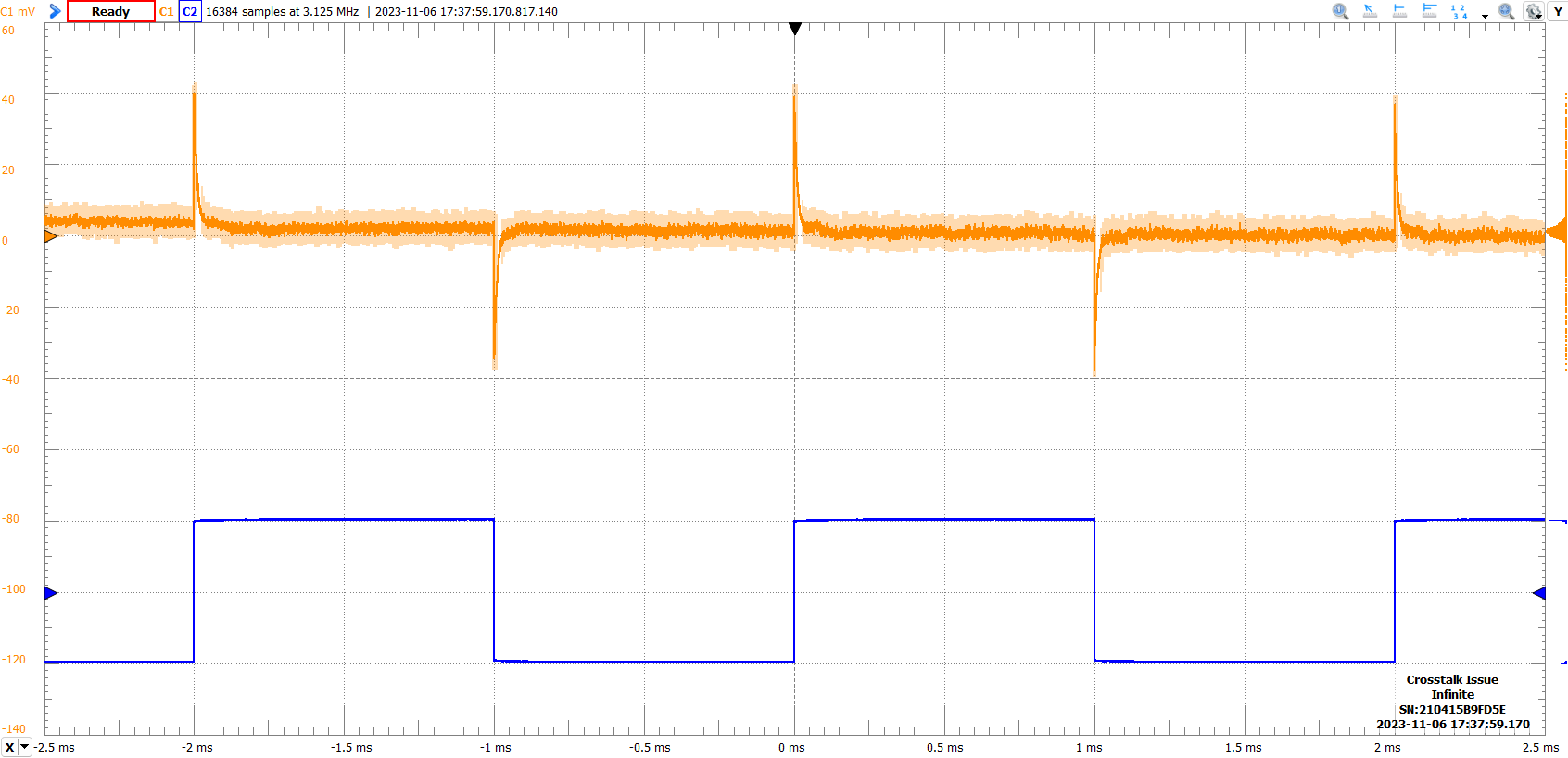
Unfortunately, this is where it started to get really bad. It became clear as soon as I fed in a square wave to one channel while having the other one on screen, that there was a serious crosstalk problem.
And this is why shielding cans are a thing.
Crosstalk
To attempt to see what exactly was causing this crosstalk issue, i.e. was it poor routing? Lack of shielding? Something else? I took 2 measurements, one with channel 1 connected to a square wave, channel 2 left open; and the other with the channels swapped.
The idea was that maybe the output of the channel 2 opamps are coupling to the inputs of the channel 1 opamps, since channel 2 is physically further from header that interfaces with the Analog Discovery 3.
If this were true, when channel 2 is the aggressor, the crosstalk should be a lot worse than when channel 1 is the aggressor.
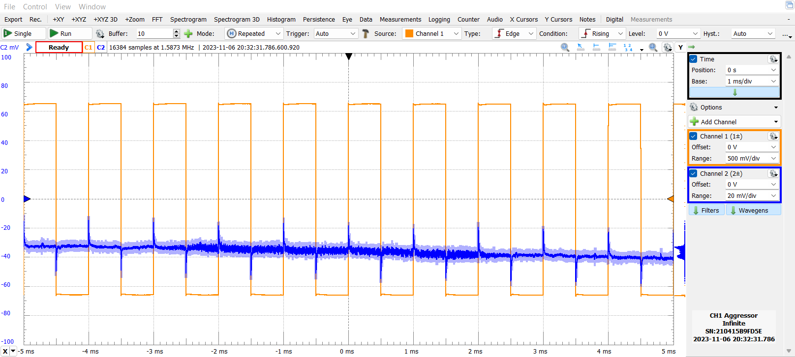
Channel 1 aggressor, channel 2 victim
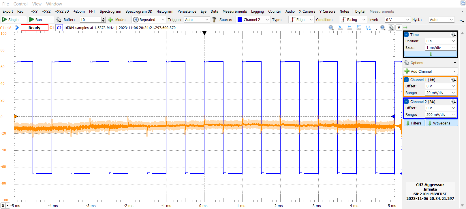
Channel 2 aggressor, channel 1 victim
The results certainly didn’t seem to support the initial guess, in fact it’s almost as if they are opposite to the initial guess!
Next, I shorted the input of channel 1 by connecting a probe to it and shorting the end of the probe, with channel 2 still acting as the aggressor:
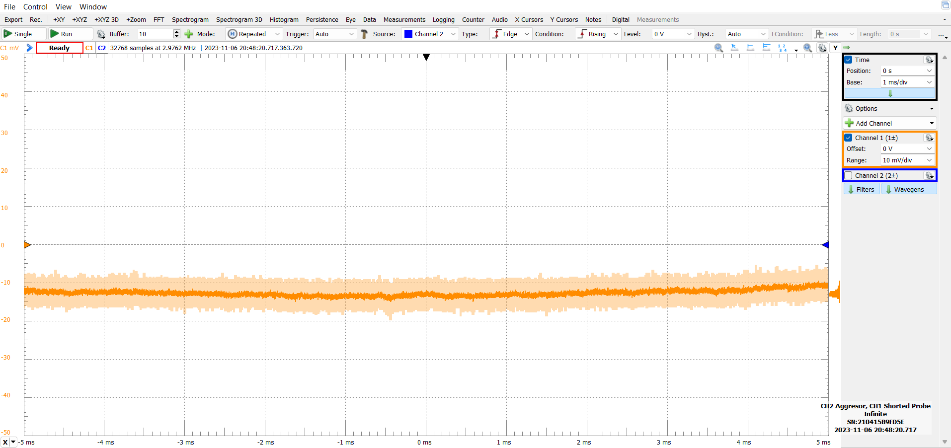
Channel 2 aggressor, channel 1 victim; channel 1 connected to shorted 10x passive probe
Lo and behold the noise was completely gone, despite the short being at the end of the 10x probe and not directly on the board!
Why the on board 1MΩ termination resistor to ground couldn’t do this on its own is beyond me.
But one thing is crystal clear though: this board needs shielding. I’ve never worked with these higher speed CMOS opamps before, and never would have thought noise pickup would be such a big problem. What a great learning experience!
This is made even more clear when I put my hand a few inches above the board, not touching anything:
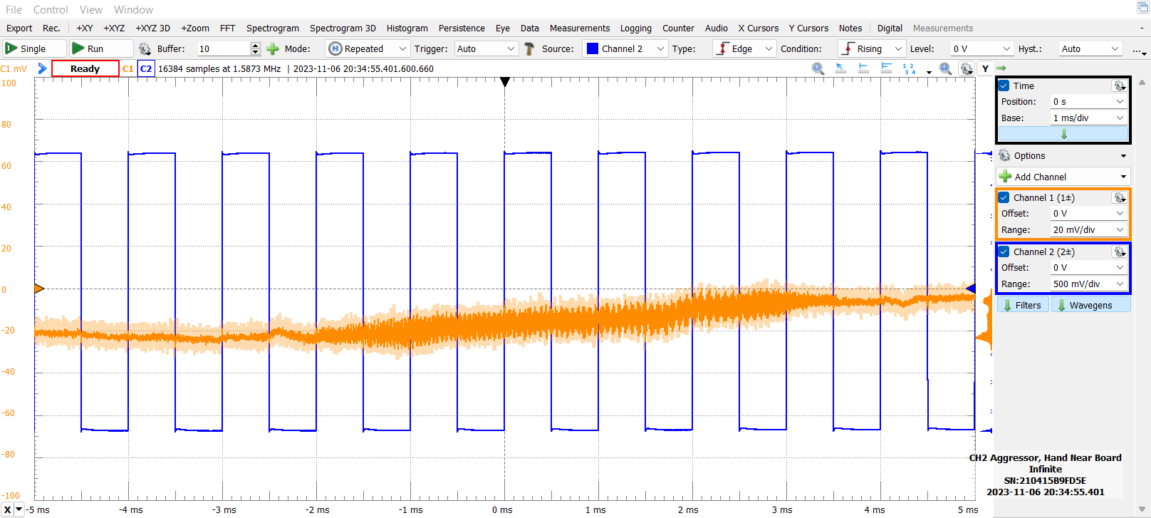
Channel 2 aggressor, channel 1 victim; channel 1 BNC not connected to anything
The pickup just due to that completely swamps out the crosstalk! That was absolutely crazy to me.
Noise pickup
With nothing connected to the input BNCs, the output of the amplifier had this spectrum:
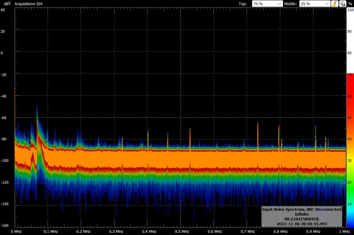
Noise spectrum with nothing connected at the input
I wonder what is that weirdness at around 70kHz, on the real time spectrum it came and went, almost like wireless data packets. Hmm…
That aside though, look at all those spikes. Yikes!
With a probe connected to the BNC, I got this:
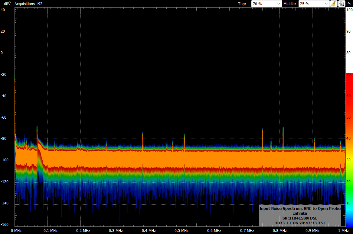
Noise spectrum with a probe connected
Basically it’s the exact same thing, so I think it really is the board needing shielding, instead of the probe acting as an antenna or anything like that.
Shorting out the probe with the usual long ground lead proved this hypothesis, since the noise was basically gone, despite the huge antenna loop at the end of the probe.
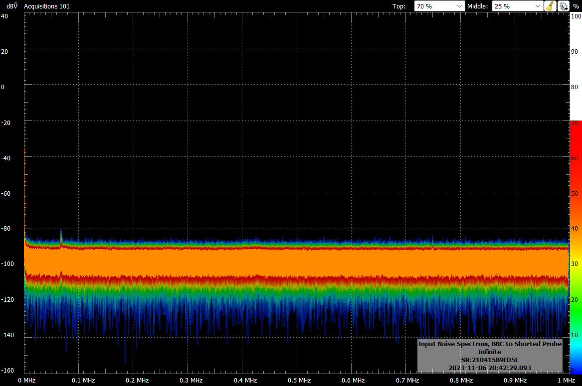
Noise spectrum with a probe connected; probe shorted to ground
Build notes
The first time I powered up the board, channel 2 had a really really bad offset problem:
After some sleuthing around and measuring stuff, I ruled out the basics like supply ripple or board contamination (flux residue), and narrowed it down to the main amplification stage opamp which had the unusually high offset voltage.
I even tried retouching all solder joints around that opamp, still no luck.
Measuring the input resistance of non inverting input of the main opamp in channel 2 provided some clues. When the board was powered off, it measured 1MΩ as expected. When the board was powered on though, it immediately dropped to 700kΩ.
Moreover shorting the input cleared this offset voltage.
It was as if there was something pulling the input node high… My mind immediately went to the tendency of semiconductors to fail short. Maybe, just maybe, this particular opamp got zapped by ESD and somehow something inside it had gone Lo-Z with respect to the power rail.
Swapping the opamp fixed it, so it was indeed a problem with the opamp. Whether or not it was actually ESD that killed it, I can’t say for sure, although it has been quite a wake up call since, if it really were ESD, it would be the first time I had an IC killed by ESD.
Conclusion and future changes
All in all, I think this quickie project turned out quite well!
That being said, there were definitely things that I’ve overlooked, like the lack of shielding and general component placement. Therefore, I do intend to make a second revision, with the following changes:
- Add shielding
-
Add trimmer pots to each channel to trim out the offset voltage - Add better silkscreen to the output side header, as it stands right now it’s super annoying if I want to connect anything to the output header
- Add ESD protection to the analog inputs. Bourns and AVX both have sub pF ESD protection devices (Bourns has MOVs and micro scale spark gaps, while AVX has TVS diodes)
- Better routing to reduce crosstalk
- Better silkscreen artwork so it looks nicer
Until then, thanks for reading!