I recently picked up a Behringer BA85A (yes, yet another Behringer clone…) dynamic microphone, and have thoroughly enjoyed the sound that comes out of it. However, it does require me to crank the gain on my PreSonus AudioBox iTwo audio interface all the way to the maximum, and even then, I either have to speak quite loudly or be right on top of the microphone to get a signal that I don’t have to apply any post amplification, which is kinda annoying because I use it quite a lot for video calls, and sometimes adjusting the levels for ASIO devices can be tricky.
Of course, I could have just bought a FetHead, or something cheaper like the Klark Teknik CT1. But being a Malaysian, the amount of money I have been spending in the UK just for everyday life has been astronomical, and I really didn’t feel like splurging. Plus, this is Infinus Electronics, we use excuses like this to go out and, well, splurge on buying components and fabricating stuff.
But hey, at least I get to learn something along the way!
Schematic
As always with all things audio, the very first thing I did was to check if Eliott Sound Products had anything that I could copy/modify. And, ESP being ESP, it never fails to deliver, and the all important gain stage of the circuit is based off Project 66 .
All I did was to select some low noise transistors, modify it to work with phantom power, set the gain, and design a board.
Here is the final circuit that I came up with:
Some janky description of how this circuit works
Disclaimer: I have no idea if what I’m saying here is true at all. In this case it seems to add up according to the MicroCap simulations, but really, the proper way to do it would probably be with small signal models and such.
I’m trying to learn analog design, and so I grasped this opportunity to try and work out how this circuit works.
Gain stage
When it comes to differential amplifiers, the first thing that comes to mind is the long tail pair (LTP), and indeed, this is sort of like a long tail pair, but with what I call current steal. I have tried to search high and low on Google if there is a name for such a topology, but so far, no luck at all. There is something similar on Cordell Audio (also another gem!), but that’s pretty much all I managed to find.
First, pairs Q1, Q2; and Q3, Q4 form PNP complementary feedback pairs, also known as Sziklai pairs. So, it will seem like everything is upside down compared to conventional LTP implementations online that use NPN parts.
Together, these transistors form some sort of LTP like arrangement, with the overall collector current set by R3 and R6, since the emitter has to be one Vbe away from the base voltage, which in this case is mid-rail or 7.5V.
To understand how it all works, think back to how an LTP works. it basically forces the emitters of both sides to be at the same potential. Therefore, any small change in the difference in voltage presented at the bases will cause the base current flowing in both sides to be different.
This small difference in base current is amplfied by the current gain of the transistors, and thus the voltage at their collectors is no longer the same, with a much larger differential than what is present at the bases.
Now, the way this circuit works is it does away with the strict requirement that the emitter voltage has to be the same on both sides. R5 sets the amount of difference that is permitted, and thus the greater its value the smaller the gain. C2 is there to filter out DC, which reduces the DC gain so that if whatever is plugged in to the XLR input has a DC differential voltage, that doesn’t completely swamp everything out.
To fully understand it intutively, I think it is very beneficial to try and work out all the currents flowing in the circuit, and arrive at the formulae for the gain etc. However, since I’m not using the small signal models to analyse everything, which is probably the way to do it anyway, here is just a jank back on the envelope attempt at working everything out.
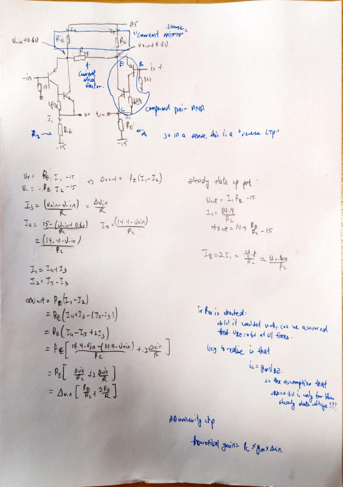
Authentic handwriting
The original ESP post used 2N4403 and BC549 transistors, however, LCSC did not have them in stock… Dammit silicon shortage…
I found this really nice page that tested a whole bunch of low noise transistors, and settled on the PBSS4540 and PBSS5540 transistors. I’m still unsure how it will compare to the 2N4403 and BC549 combo, but simulations seem to imply that they are as good, if not better, in terms of noise floor.
The outputs are AC coupled because remember, the XLR lines have phantom power on them.
Collector loading
Technically, the value of R2 plays a key role in the noise performance of the circuit, as it determines the collector current of the NPN elements. It’s value should be reassessed for different transistors. However, using the original values provided really good noise figures in simulation, so I didn’t bother investigating further.
Caveat: gain depends on the differential impedance connected to the output
I didn’t realise that this was going to be a problem until I actually ordered the boards. Essentially, because this circuit operates on currents, any current drawn by the output load will cause the gain to decrease.
To mitigate that, the original ESP circuit had an opamp buffer, but mine doesn’t so, it remains to be seen if it will play nice with my audio interface’s input impedance of 1.5kΩ.
Power supply
Once again, referencing ESP, this time the article Phantom Power - What It Is And How It Works , I tacked on a simple zener diode based regulator to provide a know supply voltage to work off of. As noted in the article, and dictated by ohm’s law, with a 15V rail you’d have 9mA-ish to work with, which is adequate for this scenario, but may not be for opamp based designs. For example, the TI NE5532 typically requires 8mA, and that can go up to 16mA.
Of course, nowadays there are a lot of really nice, low noise and distortion opamps that use very little power. One example is the OPA1692 which runs at a cool 650μA per channel. I was going to use those to make a 3 opamp instrumentation amplifier type implementation, but guess what, they were sold out everywhere…with lead times of more than a year! Plus they aren’t exactly cheap so, discrete it is!
With the values shown, MicroCap (a nice free simulation package) says that each leg draws about 3mA of quiescent current, putting us well within the budget.
SPICE results
This was the first ever time I genuinely made the effort to simulate everything before actually designing the board and ordering the parts. This was mostly because I was curious how everything in this circuit works, and simulating it would allow me to play with it in a sort of sandbox without burning a hole through my wallet.
According to the simulation, this circuit has an RMS output noise of about 10uV, which, given the gain, translates to about 256nV of equivalent input noise. That’s an input noise density of 1.5nV/√Hz, which is mighty fine by my standards, given that the SSM2019 has an input noise densith of 0.9nV/√Hz. Distortion performance was also stellar, with any sensible input giving virtually negligible levels of distortion.
Running the simulation with a 1.2kΩ differential output load produced a flat gain of about +25dB from 20Hz to 20kHz, which was good enough for my needs. That being said, the unloaded gain was more like +35dB, so the reduction in gain due to this loading is quite drastic.
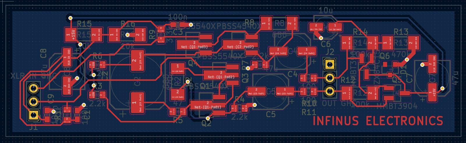
PCB layout
Believe me, I genuinely tried my very best to make it as small as possible. There are a few things that I learned in attempting this though:
- Unless you go for small packages, SMD parts really aren’t that space efficient, especially large value caps.
- Not having the luxury of routing tracks under components as with through hole makes life really complicated when you’re trying to keep path lenghts short.
- These issues are made even worse if you select hand soldering friendly footprints.
So, the takeaway is, don’t use SMD parts unless you have to.
Apart from these, the usual good layout practices like not splitting up the ground plane willy nilly, small loops, short paths and such all apply.
I’m still working on a viewer for PCB svg’s, so in the meantime, here’s a screenshot directly from KiCad.
Fabrication plan
At the time of writing, I’m still waiting for the boards and the components. I intend to house everything in either a bent sheet metal case, or a machined aluminium case.
I really hope I can achieve the latter, since I have been wanting to give milling a go for a very, very long time, and the one thing of the University of Cambridge that has really appealed to me is a lot of these really cool machines are free for us students to use.
It all depends on how much the store at the Engineering Department asks for for a hunk of aluminium of adequate size; or hunks, as I’m really, really sure I’m gonna screw something up somehow.
Conclusion
Right now, the boards still have not arrived. When they do, and after I assemble them and give it a go, there will be a follow up post detailing how it all works out, plus some tidbits on making the enclosure and such.
I learned a lot going through this relatively simple circuit and trying to figure out how it all works, and playing with it in MicroCap. Really, next time you see an interesting circuit, try to identify its topology and figure out how it works, it’s absolutely worth the time, effort, and frustration, take this from someone who has been blindly copying circuits for years!
Once again, if Rod Elliott were to suddenly appear before my eyes, I would bow like a true asian to him. All the knowledge and inspiration that I got from following his site for years now, just, absolutely priceless.
Thank you for coming along this journey.
References
These are awesome and inspiring, highly recommend that you give them a read!