Introduction
The world of digitally controlled switchmode power supplies has always held a certain allure for me: the idea that you could sample things like output voltage and current, apply some DSP techniques, and then based on that output a gate drive signal in real time, giving you whatever response you want out of your buck/boost converter just seems so… insanely cool.
That being said, a lot of times these require a good understanding of the control loop architecture and parameters of switchmode power supplies to be able to properly stabilize, which has proven to be quite the barrier to entry. See the Opamp Based Boost Converter project for a bit more on what could go wrong.
Well not this time.
The constant on time control loop literally requires no loop compensation at all, it really is just sampling the output voltage and firing off a pulse of fixed width (hence the constant on time) if the instantaneous voltage is below the setpoint.
Even the old and slow MSP430 has no problem handling it.
Schematic
Full Schematic Power Stage Schematic
Full design files can be found here on GitHub .
This is essentially a buck converter, with additional gate drive circuitry to properly level shift the PWM output from the microcontroller to be compatible with the P-Channel MOSFET, and also to provide a strong drive capability to properly turn it on and off.
C101 acts as a “speed-up” capacitor, pushing more current into the base of Q101 to try to speed up the transition times, while reducing the load on the MCU I/O pin once turn on amd turn off has been achieved.
Q103A and Q103B are a complementary pair together within a single package, and provide quite a nice and compact gate drive solution.
Code
| |
The code for this project cannot be simpler. Apart from the usual setup code, it just loops over a simple routine, comparing the current output voltage from the set output voltage, and firing off a pulse if the output is low. This has the effect of sending a packet of energy to the output, increasing the voltage ever so slightly and thus achieveing regulation.
An interesting tidbit is that the ADC is set to continuous sampling mode, with no regard paid to whether or not the result register, ADC10MEM has been updated every time it’s value is polled. The reason for this is to match the behavior of the code as much as possible to the control loop simulation in the next section.
The constant on time is implemented very simply with a hand-tuned delay; while the minimum off time is provided by the time it takes to execute the rest of the code. All in all, it gives a maximum duty cycle of about 75%.
Control Loop Architecture and Analysis
The first proof of concept for this project was established in PLECS, which is very very similar to Simulink.
Control loop setup in PLECS.
First of all, the constant on time topology relies on the output ripple to achieve control. Another way to think of it is that the PWM ramp you’d see in typical switching converter control loops is literally the output ripple itself.
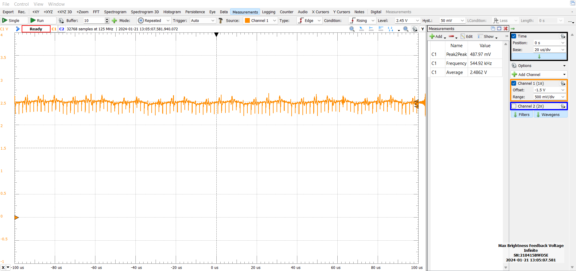
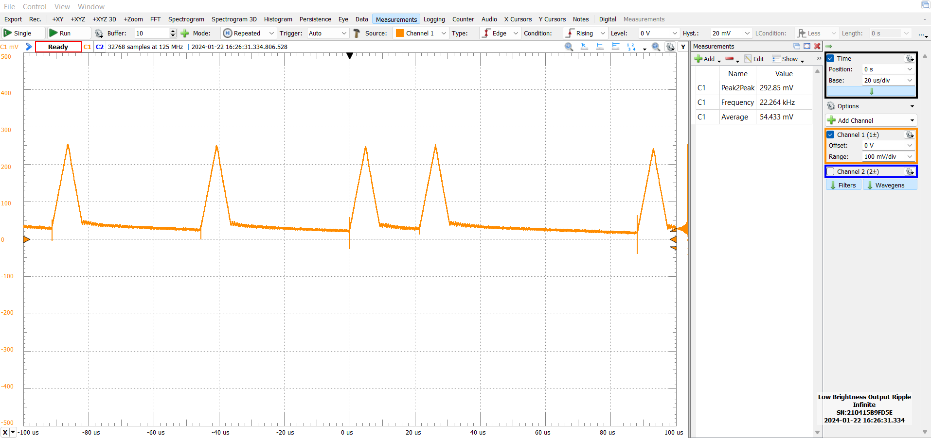
Therefore, by definition there has to be ripple at the output. In the board that I put together, at full brightness, the ripple is approximately 400mV peak-to-peak. Ordinarly this would be unacceptable, but for this LED dimming application, there was absolutely no perceptible flicker and thus I deemed it good enough.
Measured output voltage ripple at maximum brightness PLECS simulated output voltage ripple at maximum brightness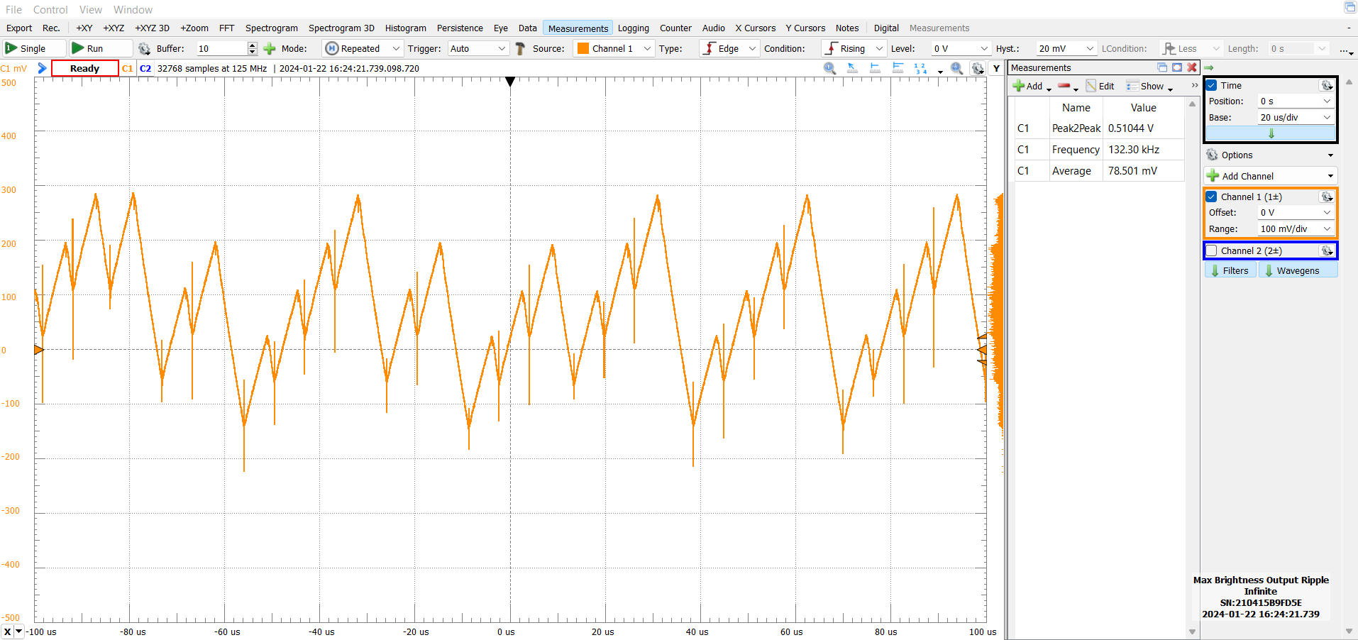
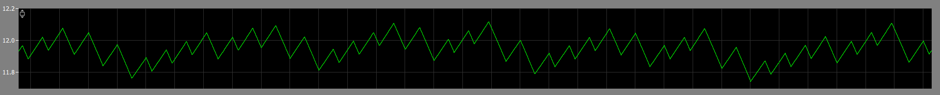
A divided down version of this ripple is presented to the ADC of the MSP430.
Measured feedback voltage
The shape and amplitude of the two waveforms is remarkably similar, which I was really pleased with because it meant that there wasn’t anything egregiously wrong with the simulation and the implemetation of the control loop in the code above, even though the sampling rate of the MSP430 ADC and the ZOH in PLECS aren’t exactly similar
I also spent a lot of time tuning the component values to try to minimize turn on overshoot, which could get pretty bad with certain combinations.
With the component values shown above, the voltage ramps up nicely with absolutely no overshoot.
Measured transient response at turn on PLECS simulated transient response at turn on. From top to bottom: output voltage, PWM out, ADC reading, inductor current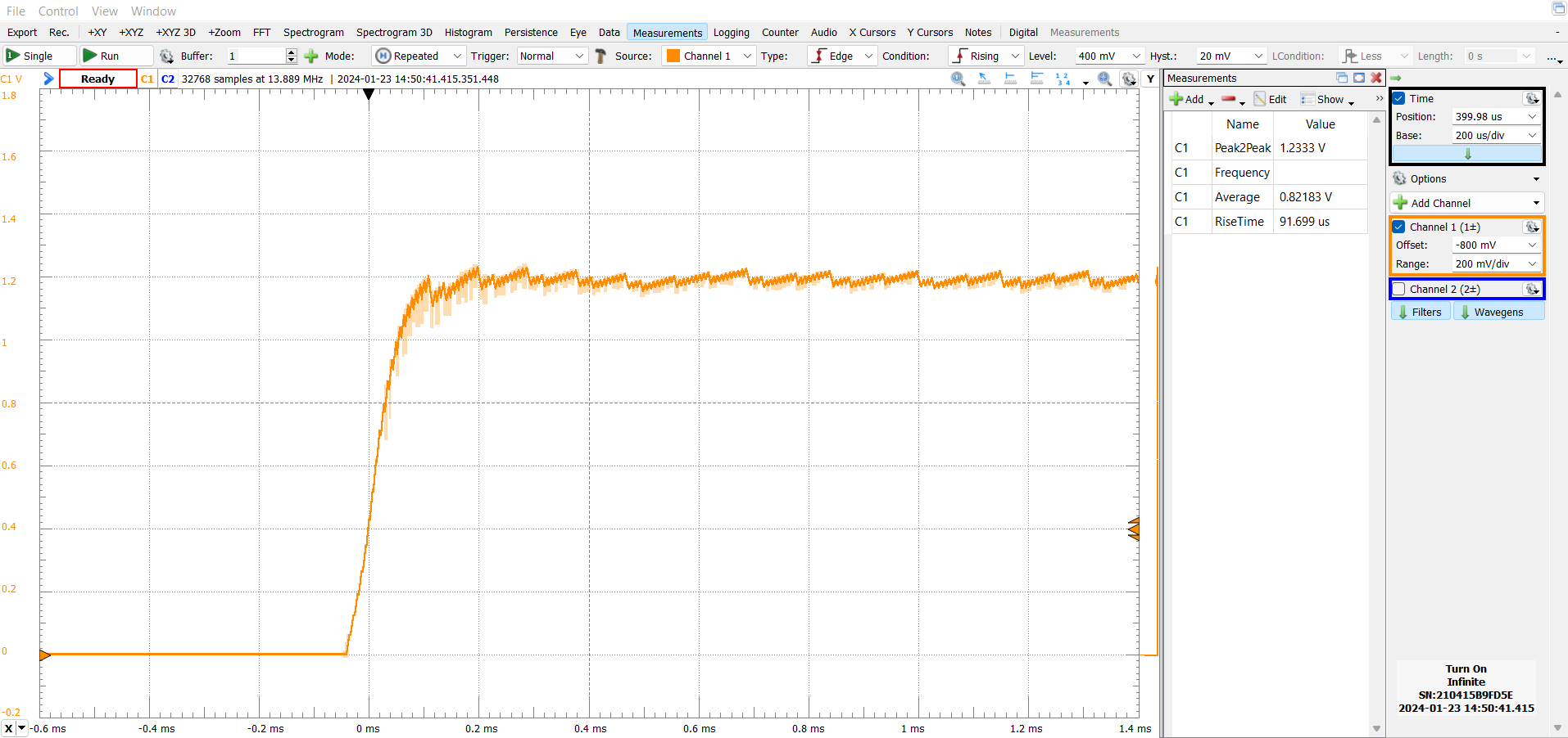
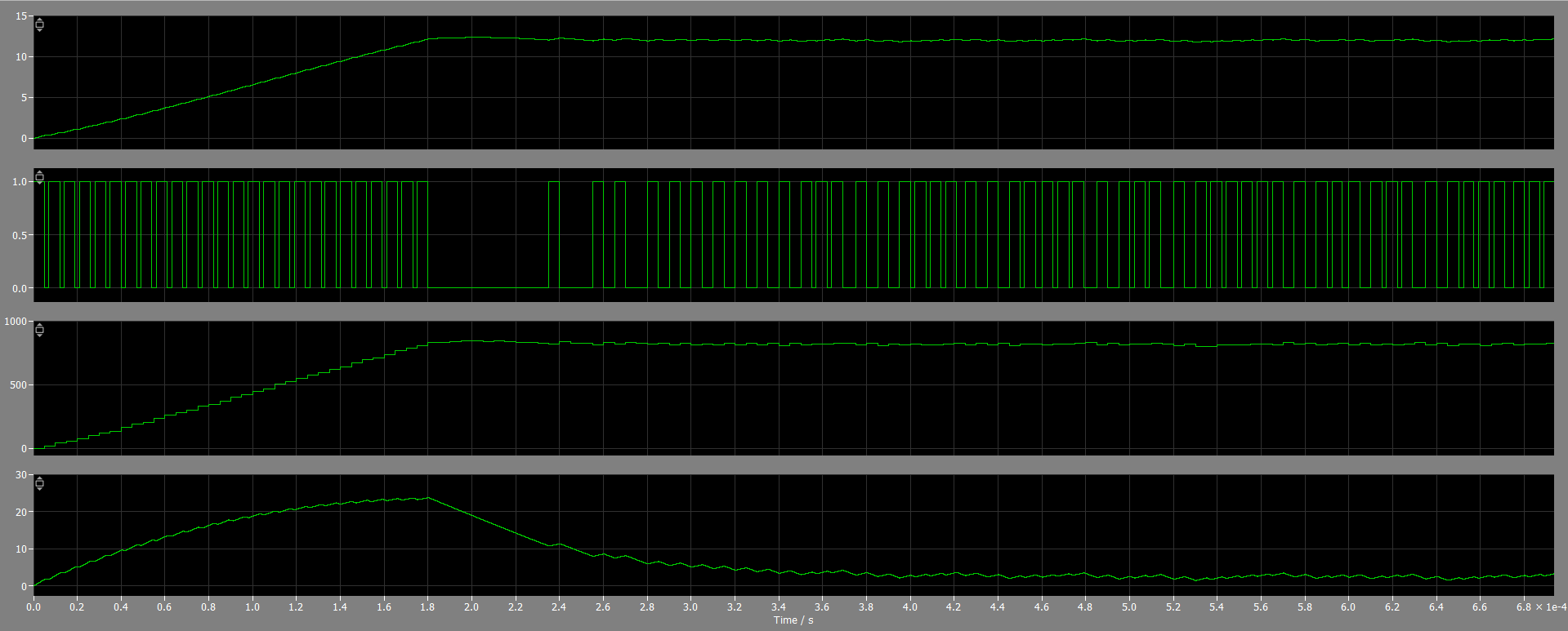
The load transient response of this circuit is also pretty good. This is what happens when I switch between the minimum and maximum brightness settings.
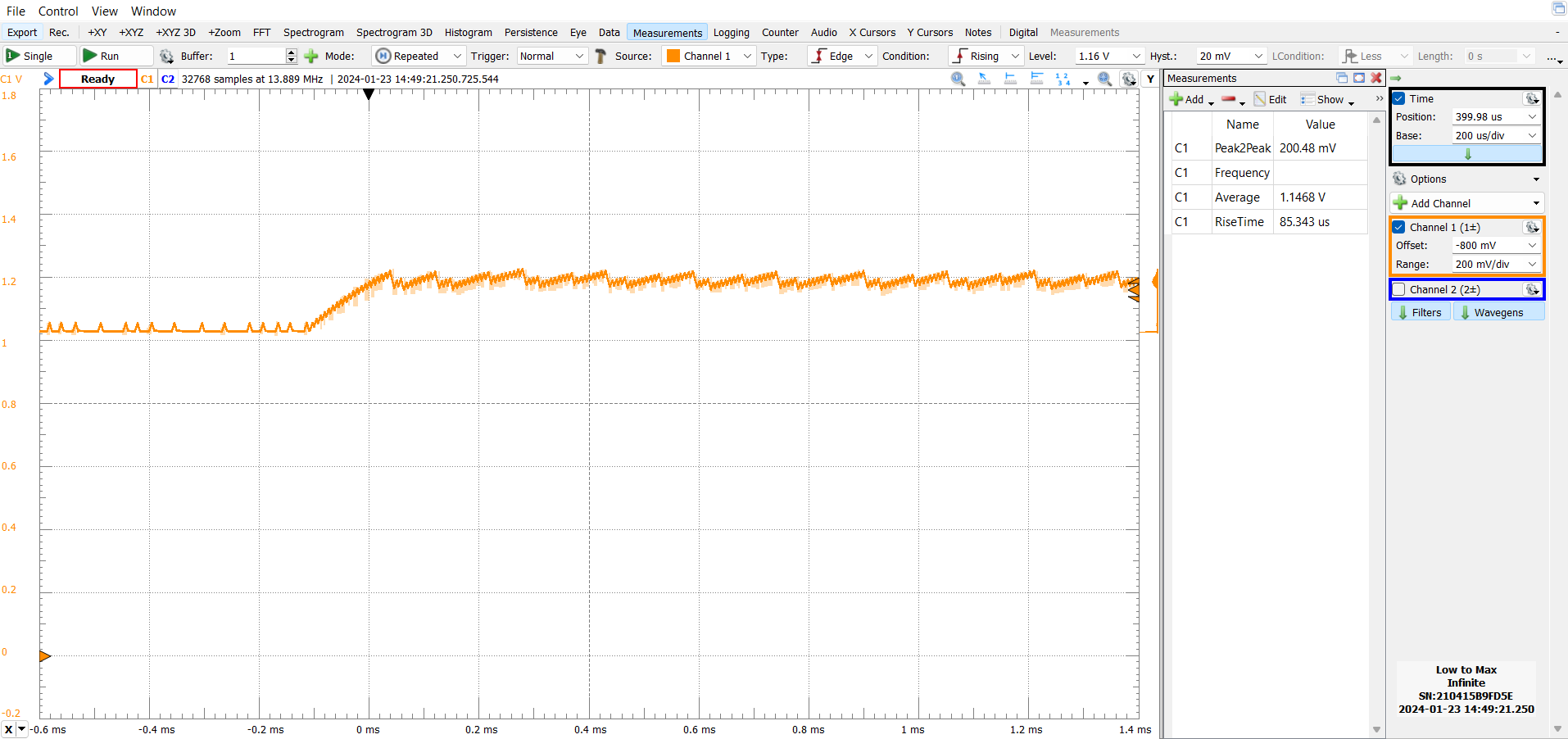
Output voltage behavior when changing brightenss
Power Stage Performance
This is probably the first time I really sat down and thought through the design of the power stage. So I had some fun measuring its performance.
First of all, when looking at the transition from low brightness to max brightness, it’s interesting to see that the ripple has different shapes in both.
Output voltage behavior when changing brightenss
Note that at low brightness, the output voltage is mostly steady, with the occasional spike. This is because the converter has entered discontinuous current mode (DCM). In fact, this behavior, with the seemingly random pulses, is similar to pulse skipping in some of the switchmode converters out there that handle very light loads.
Measured output voltage ripple at low brightness
When examining the gate drive voltage and the switch node voltage (marked SW in the schematic) at low brightness, there’s the characteristic DCM ringing.
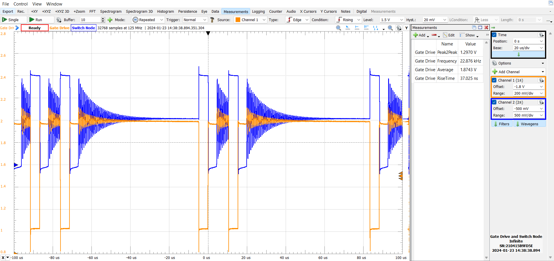
Gate drive and switch node waveforms with DCM
For completeness, here are the same two waveforms at full brightness aka continuous conduction mode (CCM).
Gate drive and switch node waveforms with CCM
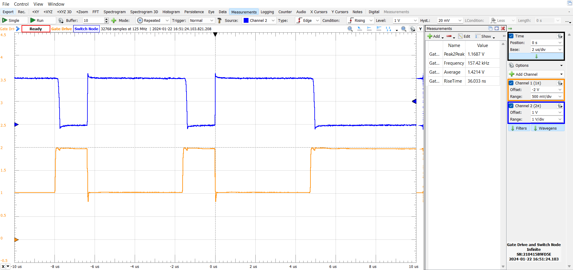
Looking closer at the CCM waveform above, there is a peculiar blip in the gate drive waveform (orange) during turn off. I later confirmed this blip to be present in both DCM and CCM scenarios.
I suspect that this is due to the charging of the P channel MOSFET Cgd, although I currently have no way to verify this.
When zooming in, things become more weird because there is not an insignificant amount of delay between Vgs falling to 0 and the rise of Vds. This might be because the current from the diode has to commutate to the MOSFET before the voltage in the switch node can rise. In other words, it is limited by the di/dt.
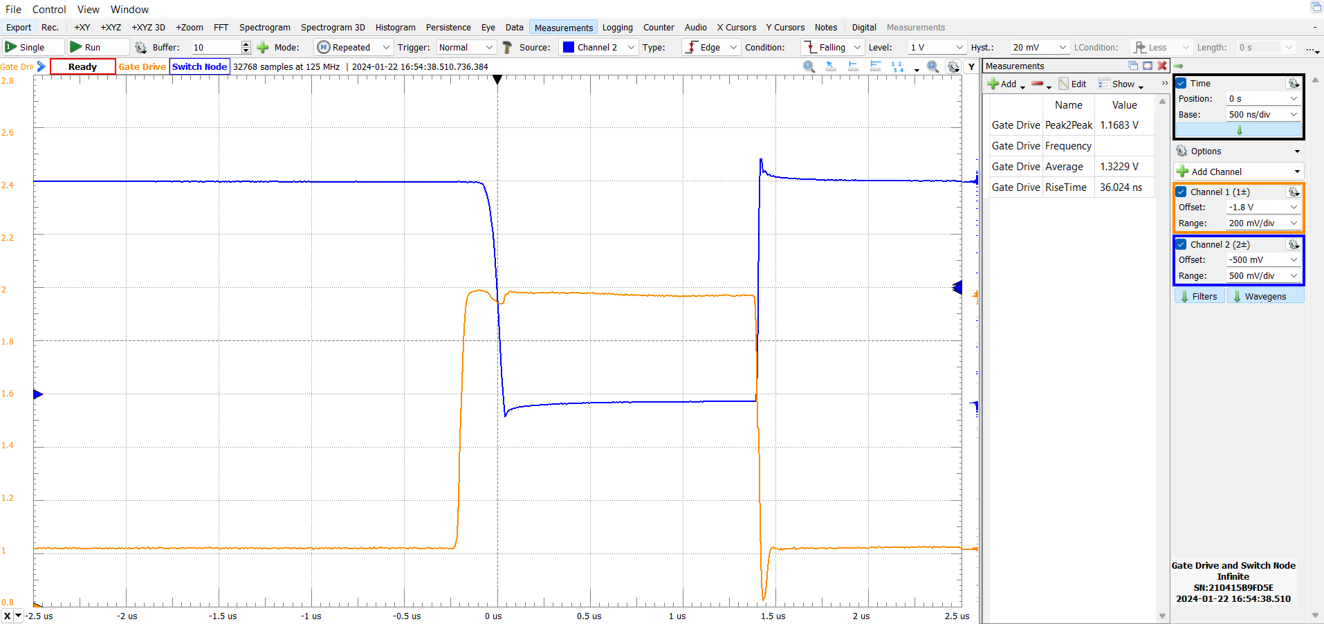
Gate drive and switch node waveforms with CCM
This is sort of strange tho, because the diode is, in fact, a schottky diode, and I don’t think it takes so long for the current to drop to zero.
More clues against this theory arise in DCM, when the diode current is, by definition, 0. In this mode, the exact same delay and blip occurs.
And for whatever reason, it doesn’t occur during turn on.
And in fact, I just couldn’t recreate this in simulation, so yeah, I genuinely don’t know what is going on. Please do get in touch with me if you have any ideas!.
On closer inspection of the datasheet, it seems like the turn off delay of this PXP015 is quoted as being 58ns, compared to the turn on delay of just 4ns. This is on top of a 58ns current rise time. The delay in the waveforms above seem to be much greater than this, but maybe this is part of the reason.
Conclusion
Well, this project proved to be a much bigger success than I thought it would be. It now powers an LED strip in my dorm room, which acts as my main source of light at night.
Only thing now that is left to investigate and fix is the annoying coil whine that this thing gives out…
As always, thanks for reading along!
Gallery
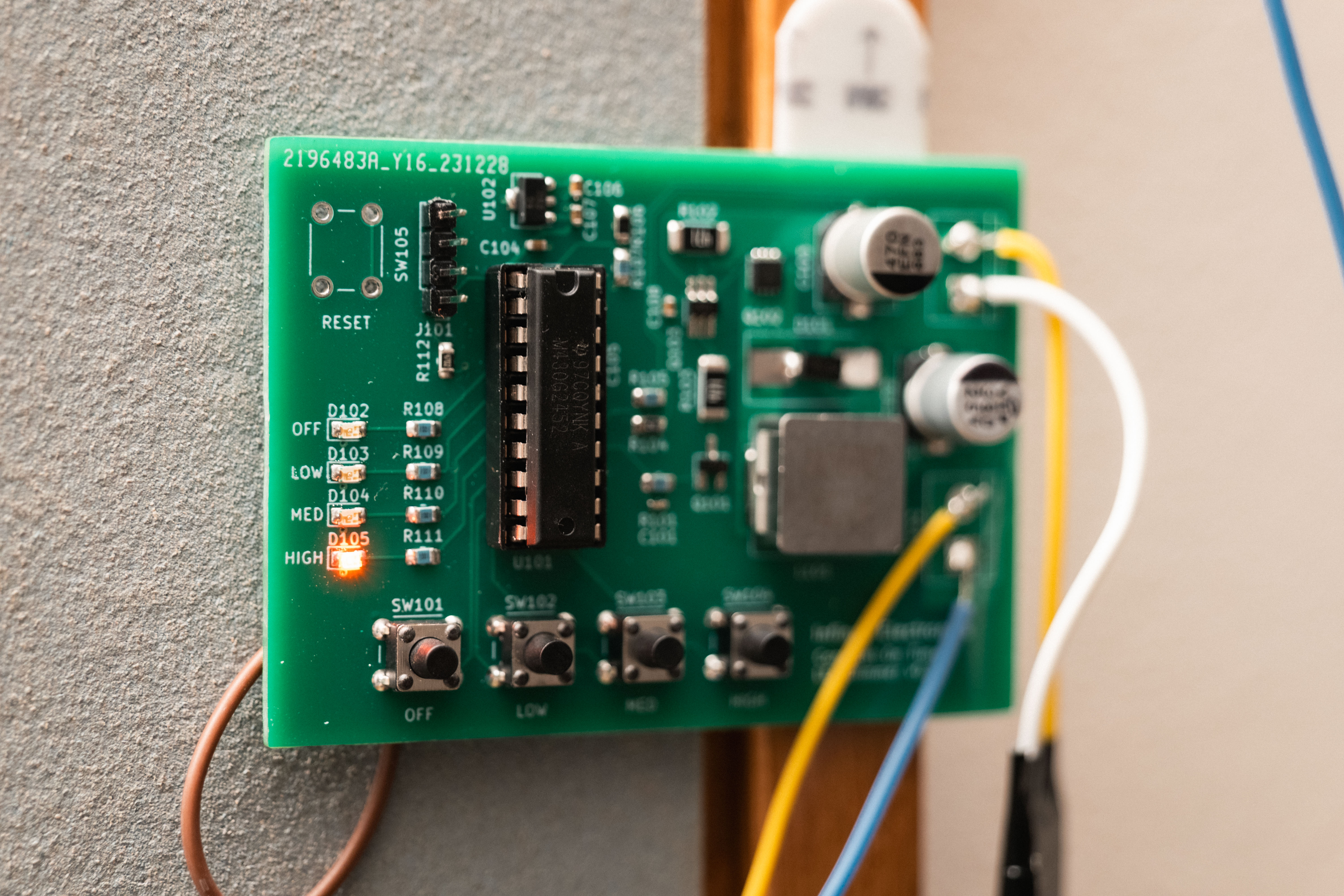
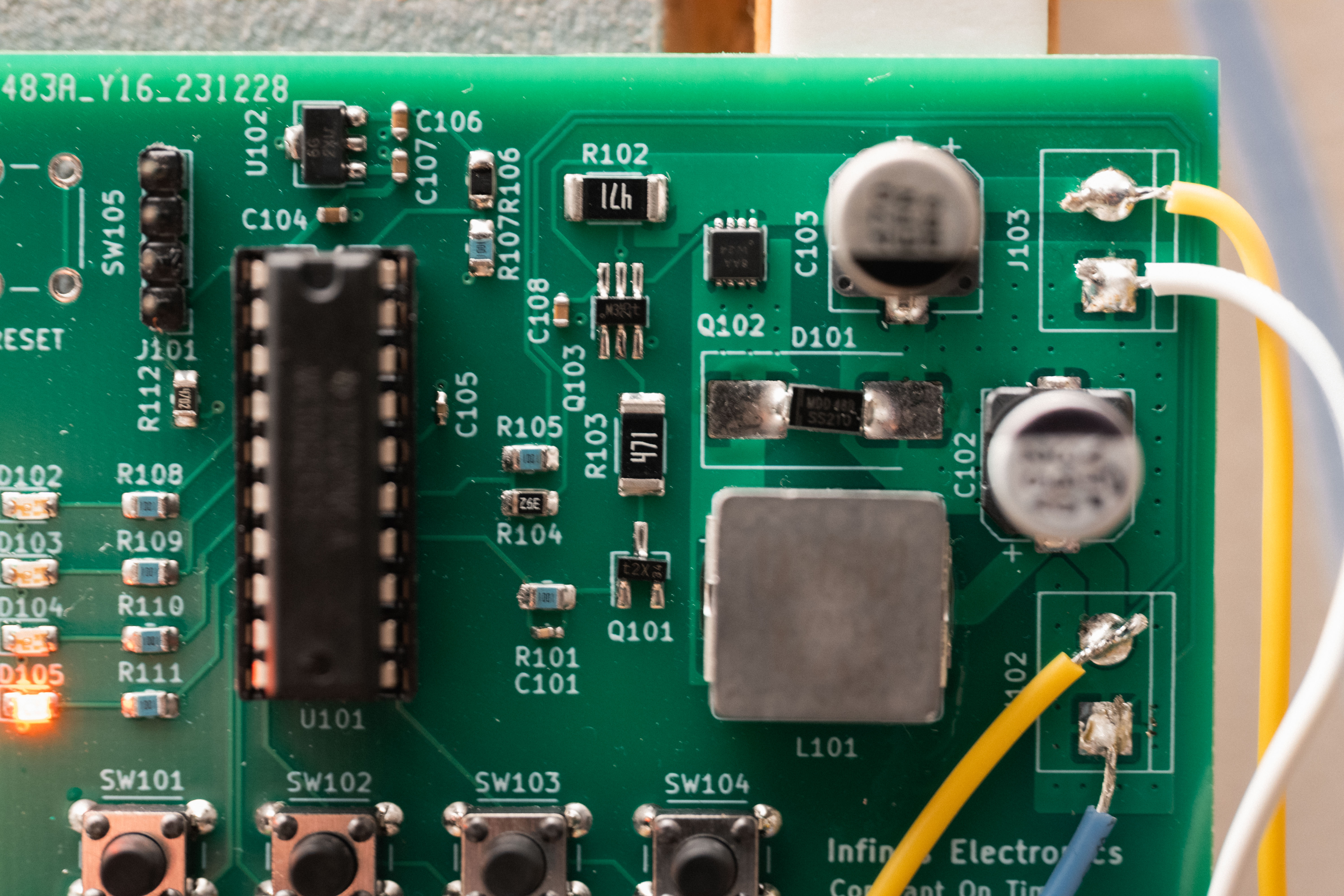
Yup, nothing like a little good old DIP micro on a board that has a DFN elsewhere 🤣 Power electronics components, with a woefully undersized diode