The good, and perhaps bad, thing about passions and hobbies is that the energy to zealously pursue them ebbs and flows as the days, weeks, months or even years go past. Just recently, I experienced a strangely strong desire to just go out there and design something again out of frusration over what we’re “learning” at university, so here we are.
Preface: Why LCSC
Because DigiKey/Farnell/RS wouldn’t give me free shipping until I spent tonnes of cash, and even then, the VAT here in the UK is just crazy… It’s times like this when I really, really miss being in Malaysia.
I also wanted this to be an experiment for myself to see just how far I could go using cheaper Chinese parts, and that includes the IC’s as well as passives. On top of that, it’s pretty much impossible to get SPICE models for these Chinese IC’s, so it would be interesting to see just how well thought out their datasheets are.
Boost converter
Topology
There were a few options when it came to the topology of the boost converter, the choices being somewhat more limited because I was trying to get boost the voltage by almost 10x (5V-ish to around 50V), and the final output had be low noise, since it would be connected directly across the signal lines of a microphone preamp. Yes, the noise will be common mode, but that isn’t to say that we should at least try to minimise it.
From researching online, a few standout options were:
- Conventional boost converter, with a voltage multiplier stage at the end
- Conventional boost converter, with a transformer instead of an inductor to more easily achieve higher boost ratios
- Flyback converter
I really wanted to try out a flyback topology, since I have not played with any of those before, and this would be the perfect excuse to get my feet wet. However, on realising just how much of a pain it was going to be to get the magnetics for that, and the transformer based boost converter, done right, I ultimately chose to go the voltage multiplier route, inspired by the TPS61170’s datasheet .
On top of that, it was vital that the boost converter operates at high frequency to shrinkify the passives needed. This project is actually a stepping stone towards a more complex build I have in mind: a portable 4 channel podcast recorder, and so it has to be as small as possible.
When it comes to selecting a topology, I found TI’s Webench Power Designer to be massively helpful.
Boost converter selection
Basically what I did was go on LCSC, selected my frequency range (I just arbitrarily chose anything above 500kHz), set the list to sort by ascending price, and go through everything one by one. As is typical with Asian semiconductors, everything seems to be inspired by everything else, which in turn is inspired by parts from the west… oh well…
I finally landed on the SHOUDING SB6286 , which has a switching frequency of 1.2MHz, which is the same as the TPS61170, and so I figured would be able to use somewhat similar values for the supporting passives. This chip clocks in at a cool USD 0.25 (dang) in 10+ quantity, so naturally, I ordered 10 of those.
It is interesting to notice that a lot of these low cost Chinese integrated boost converter IC’s do not have a compensation pin, so it remains to be seen what that would mean for the stability and transient response of the converter.
Capacitance multiplier
Then, there comes the issue of removing as much noise from the output as possible. There are, once again, a few options:
- Linear regulator
- Zener regulator
- Capacitance multiplier
In order to not waste any more power than is absolutely necessary, I chose to use a hybrid of a capacitance multiplier and a zener regulator. The circuit is designed in such a way to make experimentation easy, as I can, for example, just have a pure capacitance multiplier by omitting the zener diode altogether.
Schematic
Now, taking a look at the schematic, it all falls into place. The boost converter section is pretty much a direct copy of the typical application circuit from the datasheet, and I used the biggest suggested inductor value to try to reduce ripple current.
What follows is a voltage multiplier stage, taken right out of the datasheet of the TPS61170.
Q1 and the components around it form a capacitance multiplier/zener diode regulator. Note that even though some of the component values have been specified and others not, this circuit is intended to be customised to suit your needs, and thus, your required componenent values will certainly be different from mine.
PCB Layout
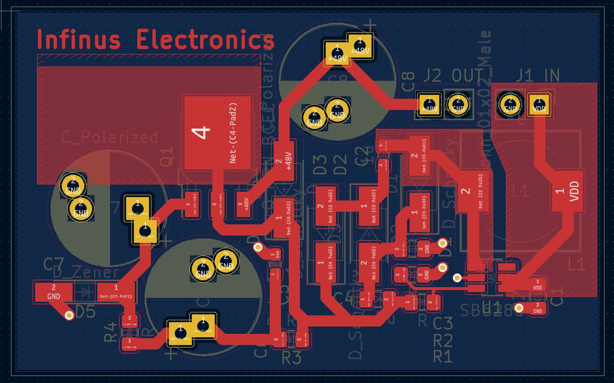
For a switching converter intended to be used as part of a noise-sensitive system, ensuring that low noise layout techniques are observed is paramount. Now, I’m not saying that I know what I’m doing here, but I did try my best to keep loop areas as small as possible and to minimise cutting up the ground plane to reduce radiated emissions.
Do check out the GitHub repo for this project to learn more about the PCB layout.
I used this interesting dual footprint for the capacitors that I found in the KiCad 6.0 footprint library. From taking a quick glance at LCSC, it seems like most, if not all, 50V capacitors from 220uF to 1000uF should be able to fit, so you can experiment to your heart’s content.
Conclusion
The boards and components are now on order from JLCPCB and LCSC respectively, until then, the performance of this little circuit remains to be verified. I had a tonne of fun combing through the smorgasbord of weird and wonderful components from LCSC, and the afternoon I spent glued to my computer coming up with this design was a much needed departure from the slew of random stuff we are being made to study.
Until then, thanks for coming along the journey!