Introduction
I started off this project when I realised that the official Discovery BNC adapter board has too high an input capacitance to be used with generic scope probes, which usually have a compensation range of 5-35pF ish.
Using scope probes is really necessary in some cases where low loading is desireable, since the quoted 1MΩ || 24pF input impedance of the Analog Discovery 3 loads down sensitive analog circuits quite significantly. Also, the plain jumper cables supplied aren’t the best for signal integrity.
The front end amplifier module presented below enables the use of typical x10 oscilloscope probes with the Analog Discovery 3, and brings about some usability improvements too such as:
- Switchable 10x attenuation, ie common mode voltage range of almost ±5V to ±50V
- Switchable AC/DC coupling
If you would like a bit more context regarding how we got here, do refer to the MK1 and MK2 articles in this project series, it’ll make some of the points discussed below make a lot more sense.
Schematic
Full design files can be found at this project’s GitHub repository here
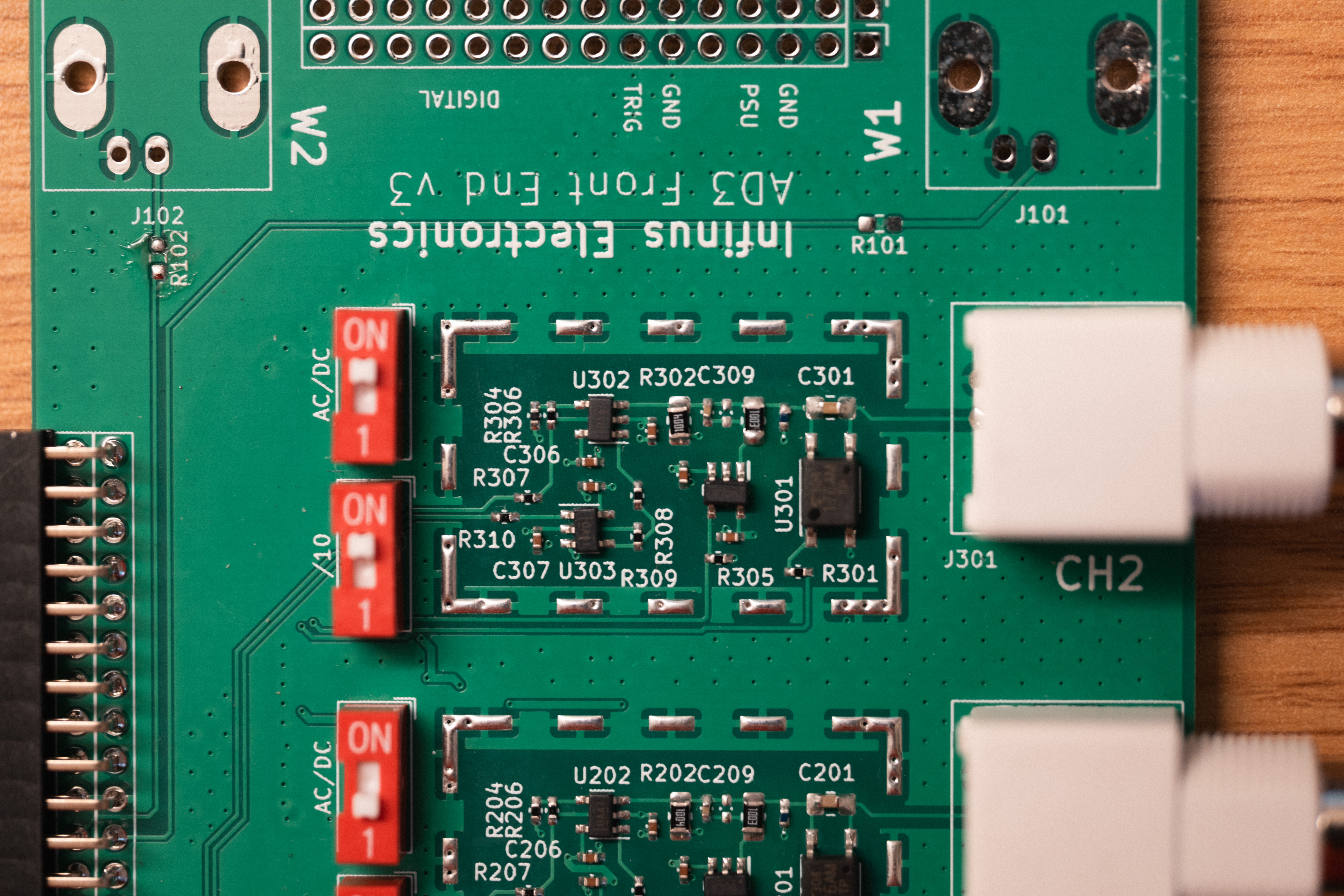
At the heart of the circuit are two OPA356 CMOS opamps, which are directly responsible for the great performance of this front end. U202 provides the nice low input capacitance, and provides the bulk of the gain; U203 inverts the output of U202 to achieve a differential output to drive the differential inputs of the Analog Discovery 3. The gain is needed to make up for the 10x attenuation when using a x10 scope probe.
Low-ish value feedback resistors are used to provide a nice flat gain response up to 70MHz (simulated). Using higher values will result in peaking before rolloff.
U201 is a photorelay, i.e. solid state relay with input to output galvanic isolation, and is responsible for bypassing the AC coupling capacitor if so desired. The isolation is nice because it provides minimal capacitive loading at the input: the TLP176AM is rated for 0.8pF.
R203, C203 and C209 form an additional 10x frequency-compensated attenuator. IC201 engages or disengages this additional attenuator, giving 2 selectable input ranges. The value of C203 was selected by trial and error on a completed board to give the most similar pulse shape between the two ranges, eliminating the need to recompensate the probes when switching between them. C209 is there to allow additional fine tuning, and was unnecessary in my build.
Shielding
Shielding cans are absolutely essential in a circuit like this as the high input impedances pick up a lot of noise from the surroundings. I used pre-made shielding cans from Mouser, but to save cost, you can probably fashion something out of sheet brass or copper.
Power Supply
Positive and negative LDOs are used so that we don’t lose the ability to adjust the output voltage of the Analog Discovery 3’s bipolar supplies. Pi filters are also added for good measure, just in case the supply outputs of the Analog Discovery 3 are noisy.
0402 1uF capacitors are used throughout for the best filtering performance, as these packages have low inductance. Yes, they’re quite challenging to hand solder, but with a lot of patience, and flux, they’re not too bad.
Alternatively, use a cheap mini reflow hotplate from AliExpress and solder paste. At the time of writing I just got myself one for approximately GBP20 and it has been a huge game changer for doing SMD work.
Performance Evaluation
Compared to the MK2 , the general performance of this MK3 front end has been largely unchanged, which is great as it was excellent.
There is one small caveat though: it seems like the addition of the second attenuation range introduced some overshoot that couldn’t be compensated using the probe compensation alone. This overshoot is present in both attenuation ranges.
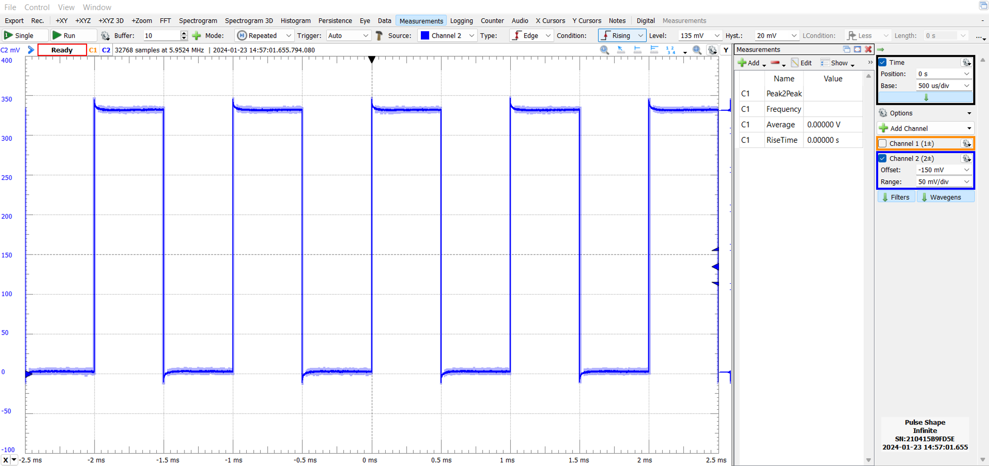
Overshoot in the pulse response.
That being said, I have not found this to be that big of an issue thus far.
Polypropylene Capacitor Shenanigans
Up until the first assembly of this MK3 front end, I used a 10n polypropylene capacitor (Panasonic ECH-U1C103JX5 ) as the AC coupling capacitor, reasoning that such film capacitors would be better for filtering applications compared to ceramic capacitors.
Well, turns out that for whatever reason, it really wasn’t AC coupling at all, and the issue described in the MK2 was present again. I was stumped for a while, until I just randomly decided to swap out this capacitor for just a generic 100nF X5R ceramic capacitor.
And just like that, everything worked as expected.
I’m still unsure why this particular film capacitor passes through DC in this application. If you have any answers, please do reach out.
Compensated Attenuator
Yet another conundrum comes in the compensated attenuator. I estimated the worst case input capacitance of the front end to be no more than 35pF (coz that’s the probe’s max compensation range). By that reasoning, C203 shouldn’t need to be much more than 350pF or so.
However, bench testing showed that a 1n capacitor was required, and even then it might need more to tame those overshoots.
So once again, if you know where I went wrong, please let me know.
Conclusion
It’s probably the first time I’ve iterated on a project, and if I could go back in time, I’d definitely push my former self to do so too. It’s just such a world of difference than just stopping right after a build has been completed; I’ve learned things that I could never have learned had I stopped at MK1.
And that’s not just in terms of the circuit design. Each time I improved on the process of assembling the board, from hand soldering to reflowing with a hotplate; and also refined my component choices to optimise on the cost of the thing.
So yeah, sometimes, it really is worth it to stick to a problem for just a little longer, even though it seems solved.
Thanks for reading!
Completed board before shield was soldered on. I chose to leave the output headers and wavegen BNCs unpopulated because I was lazy.